- Mark as New
- Bookmark
- Subscribe
- Mute
- Subscribe to RSS Feed
- Permalink
- Report Inappropriate Content
Hi,
I have used Quartus Prime Pro to design a component to write to port A of a 2-port RAM.
For port B, it is supposed to be connected to Agilex HPS h2f_axi_master, which will perform a read.
I saw that h2f_axi_master has a lot of signals.
As for port B of the 2-port RAM, it has
data_b
q_b
address_b
wren_b
byteena_b
I don't know which signal is supposed to be connected to which signal of h2f_axi_master.
Do you have the sample Quartus / Platform Designer project for such a desgin?
Hope to hear from you soon.
Regards
Link Copied
- Mark as New
- Bookmark
- Subscribe
- Mute
- Subscribe to RSS Feed
- Permalink
- Report Inappropriate Content
You're either inferring or adding a standard RAM IP through Quartus. If you use the "On-Chip Memory II (RAM or ROM) Intel FPGA IP", it has options for an Avalon or, better yet, AXI4, interface to connect to the h2f interface.
- Mark as New
- Bookmark
- Subscribe
- Mute
- Subscribe to RSS Feed
- Permalink
- Report Inappropriate Content
Hi,
I am checking on the connections diagram.
Please do allow some time to check.
Regards
Tiwari
- Mark as New
- Bookmark
- Subscribe
- Mute
- Subscribe to RSS Feed
- Permalink
- Report Inappropriate Content
Hi Tiwari,
Thanks for coming back.
I have changed to use on-Chip Memory II (RAM or ROM) Intel FPGA IP. Can you help me to check its connection to the HPS' h2f_axi_master?
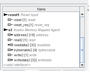
The pins on the on-chip memory's sides are
address2
read2
readdata2
byteenable2
write2
writedata2
address2, readdata2 and writedata2 can be connected to h2f_ARADDR, h2f_RDATA and h2f_WDATA respectively.
But I really don't know read2, write2, byteenable2 are connected to which pin of h2f_axi_master.
Please help.
Regards
- Mark as New
- Bookmark
- Subscribe
- Mute
- Subscribe to RSS Feed
- Permalink
- Report Inappropriate Content
Why are you trying to connect individual signals? Just add the RAM as a component in Platform Designer and connect it to the h2f interface.
- Mark as New
- Bookmark
- Subscribe
- Mute
- Subscribe to RSS Feed
- Permalink
- Report Inappropriate Content
Hi sstrell,
Thanks for coming back to me.
I did not connect individual signals.
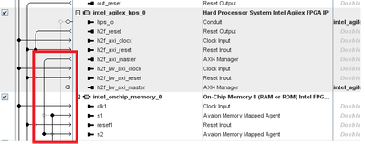
Below shows my connection between my HPS' h2f_axi_master and on-chip memory II's s2. There is no problem with it.
The problem comes when you write the code.
If you open up the on-chip memory II, you will see these signals,
When you do the coding and if you want to, say read, you need to provide read2 signal with a high signal and also you byteenable2 signanls with high (depending which byte you want to read) before you can, actually, read.
read2 <= '1';
byteenable <= "1111"; -- assuming I wan to read all the 4 bytes
address2 <= "00 0000 0000 0000 1111"; -- assuming I want to read address 0x000F
readbuff <= readdata2; -- assuming readbuff is declared as signal readbuff : std_logic_vector (31 downto 0)
As you can see here, byteenable and read2 needs to be controlled by some pins at HPS's side.
So, which pins of HPS are controlling these byteenable and read2?
Regards
- Mark as New
- Bookmark
- Subscribe
- Mute
- Subscribe to RSS Feed
- Permalink
- Report Inappropriate Content
I don't understand. You're using the HPS so you should be using higher-level code (like C using the macros created when you generate the Platform Designer system) to access the RAM. Where are you still writing HDL code for this?
- Mark as New
- Bookmark
- Subscribe
- Mute
- Subscribe to RSS Feed
- Permalink
- Report Inappropriate Content
Hi Nelky,
Yes, you need to use the c code to access the OCM/RAM from the HPS side.
For this there is no need to write the HDL code.
HDL code is needed only when there is no connection between the HPS and FPGA fabric IPs.
Also thanks to Sstrell for replying in this thread.
Regards
Tiwari
- Subscribe to RSS Feed
- Mark Topic as New
- Mark Topic as Read
- Float this Topic for Current User
- Bookmark
- Subscribe
- Printer Friendly Page

