- Mark as New
- Bookmark
- Subscribe
- Mute
- Subscribe to RSS Feed
- Permalink
- Report Inappropriate Content
Dear Intel
I think I have ran into yet another unexplainable (or not so unexplainable) problem and that has to do with the DQS/DQ groups and the corresponding hi-phy interface layer.
This is the deal: I have (had) a Cyclone V GX Starter Kit that comes with one LP-DDR2 memory IC. I had the plans to create a simple custom memory controller for it. This means, that I wanted to access the DDR memory chip through just the DQ/DQS groups only and not instantiate a full-blown memory controller using the megafunction.
I quickly learnt that it wasn't so straight forward as it looked. I started off with a clean project and instantiate through Verilog HDL modules the hi-phy atoms to shape a bare interface complonent. This worked well for the data DQS groups, the DQS/DQ x8 groups. Then, I got to the command-address bus for the memory. I deducted that this should be driven by a DQS/DQ x16 output group in order to relate all relevant command signals to the primary memory clock that feeds the memory IC clock pin.
This is where trouble started. I learnt that one of the pins on this Cyclone V GX Starter Kit wasn't even in a DQS group to begin with. It was memory IC signal CA6. In the pinout file it seems that for that pin there is no DQ function for that pin (AE9). However, on the board, the AE8 pin had been left unused that does fall within a DQS group. However, I do not want to solder two pins together on the board. Upon examining the pinout file (xls sheet from your site) I noted that this problem goes for *both* sides of the FPGA; the bottom side controller and the topside controller. Also for the topside controller, CA6 is not included in a DQS group. It's the only pin that is not in a DQS group.
Then I left this alone and went on to work on the CA bus driver of the component. This means, I initially tied all pins (12 pieses for CA0 - CA9., CSn and CEn) to the same clock from the hiphy clock buffer.
In the pin planner, I assigned the 12 bus pins to a DQS-16 group. This research was independent from the Cyclone board, just to see whether I could finish the component using pin assignments corresponding to the legend of the pin-planner.
This did not work. The fitter bugged out with various errors about unable to fit DQS-enable atoms in expected locations due to tieing pins to the given clock.
When I split up the 12 pins and spread the across two x8 groups, associating each pin to the respective DQS strobe clock for the x8 group, it worked. But this is not what I wanted. This solution would leave two independent groups, each being clocked by an independent clock. So either one clock would be the memory clock and as far as timing goes, the second set of pins would be time-aligned to its own clock rather than the memory clock.
Then I went like - Ok, so of a DQS x16 groups is not working then we're going to have the fitter perform an auto fit according to the documentation, which states that if one assign the DQS pin only, the fitter will fit corresponding DQ pins to the group the DQS pin belongs to.
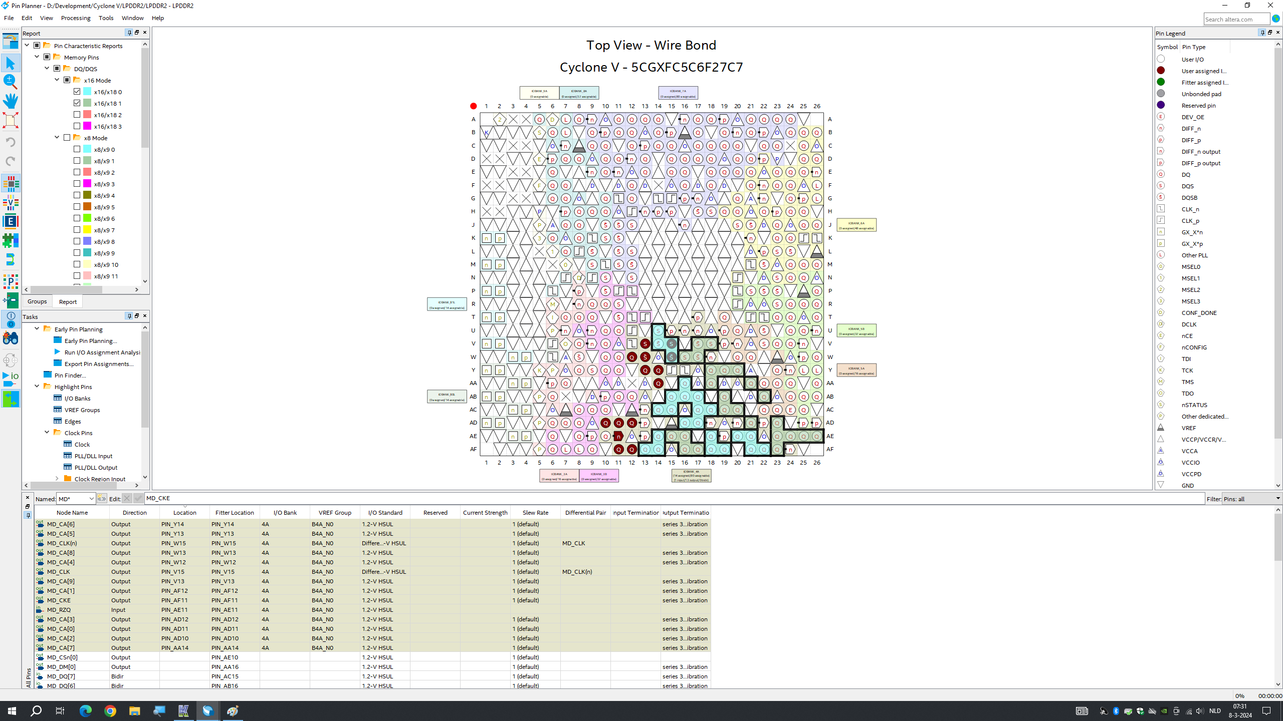
This is where things get interesting. The fitter placed the pins and the project now fit successfully, however, the auto-assigned pins did NOT correspond with the pin planner legend graphics for the DQS x16 group. You can see for yourself in the attached screenshot and you can see by loading the attached project and go straight to the pin-planner (do not compile the project). It still has these assignments. I removed the regular data group assignments and left those for the DQS x16 group only.
Then I became a bit disgruntled. And left the project for what it was. I had been thinking about whether to report it or not and decided not to. Yes, I know what's going on. It's NOT Quartus and it's not the competitor though something else instead. May be because the DDR memory was going to give my sonographer project 1.5 hours worth of memory storage of recorded audio, rather than just 5 seconds of recording time using the S-RAM on the starter kit.
Very recently, I decided to look again at my DDR interface project and loading it up. The auto-fitted pins still showed like they were on the screenshot. Again I went through the process of removing all but the DQS clock pin and have the auto-fitter fit again. I did this multiple times because:
-The fitter put the DQ pins in the opposite DQS x16 group, matching the legend.
-The fitter put the DQ pins in the first DQS x16 group, after moving the DQS pin to the opposite group.
Now it supposedly looked like it wasa fitter bug where the DQ pins were auto-placed in the opposing second group contrary to the group the DQS pin was placed in. I know it's not a bug. The random scattering of autoplaced pins as shown in the screenshot could no longer be replicated.
So to finish this report, I am going to say I now understand why you insert this liability notice with regard to downloading and using Quartus for one's projects.
Please use the attached materials for the better. So for I am not able and or allowed to use DDR memory interfaces with Cyclone V chips.
Sincerely,
Arno van Harskamp (The Netherlands)
Link Copied
- Mark as New
- Bookmark
- Subscribe
- Mute
- Subscribe to RSS Feed
- Permalink
- Report Inappropriate Content
Remark: I forgot to mention that the manual pin assignments in the attached screenshot are the copied auto-fitter pin locations. This to make the fitter pin assignments visible in the pin planner. This process was repeated for all of the tests involving the placement of the DQS pin only, where after a fit the locations were copied to make them visible as the maroon circles. This allows one to visualize the mismatch between auto-placement and the legend easily.
- Mark as New
- Bookmark
- Subscribe
- Mute
- Subscribe to RSS Feed
- Permalink
- Report Inappropriate Content
Hello Arno,
Thank you for submitting your question in Intel Community.
I'm Adzim, AE will assist you in this forum.
In my understanding, the Cyclone V GX Starter Kit has a memory component, LPDDR2 connected at IO Bank 3 and 4.
Thus the placement for this memory interface should be fixed to board schematic.
If you want to use the LPDDR2 in Cyclone V GX Starter Kit, then you need to connect the pin to those specific place as schematic.
Regards,
Adzim
- Mark as New
- Bookmark
- Subscribe
- Mute
- Subscribe to RSS Feed
- Permalink
- Report Inappropriate Content
Hello Adzim,
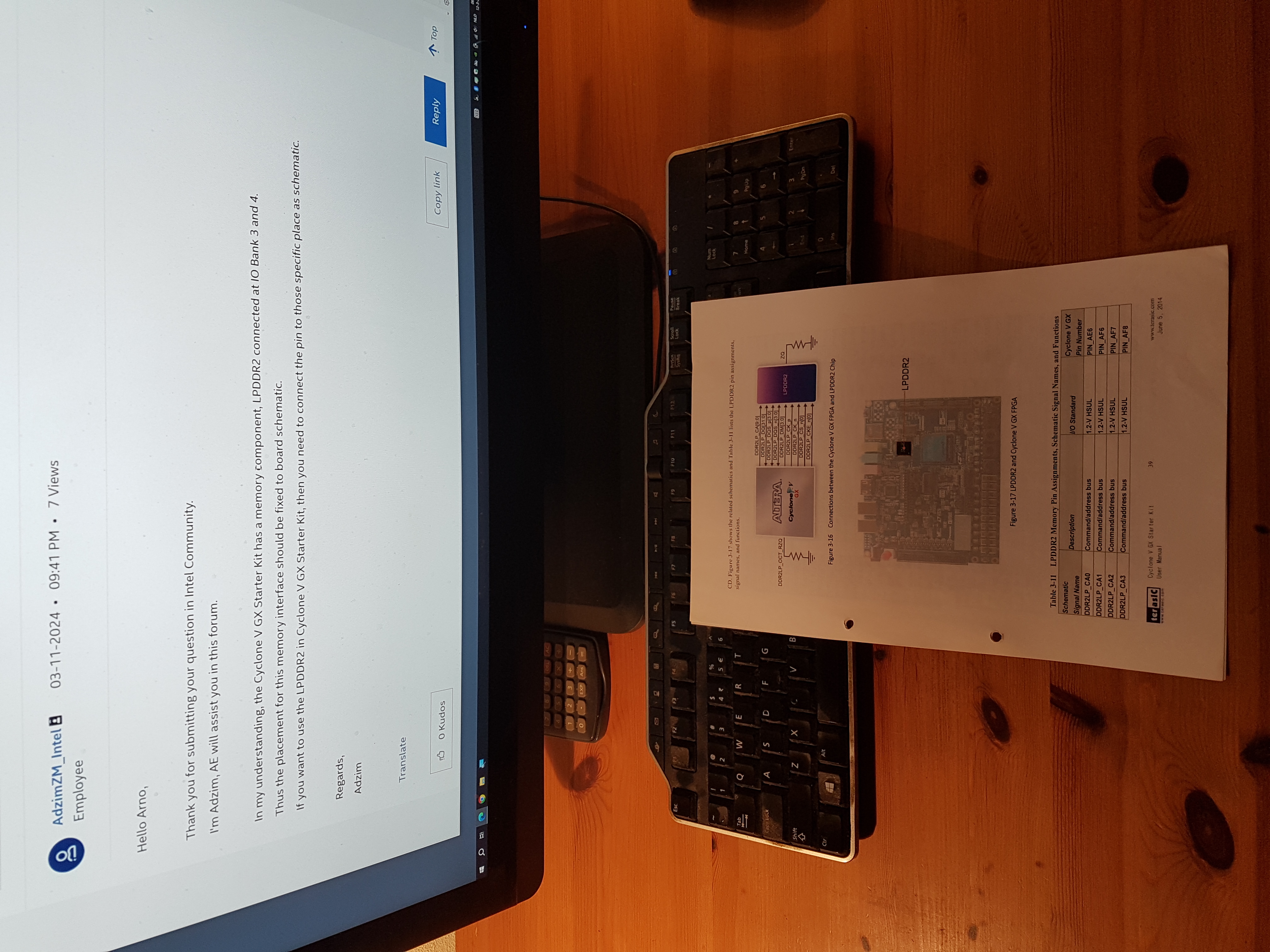
Thanks for your reply. You are right, the board has one Micron LPDDR2 4Gb chip on board. It is connected to the bottom side memory controller section of the FPGA which in actual is mounted upside down (bottom side points towards back edge of the board).
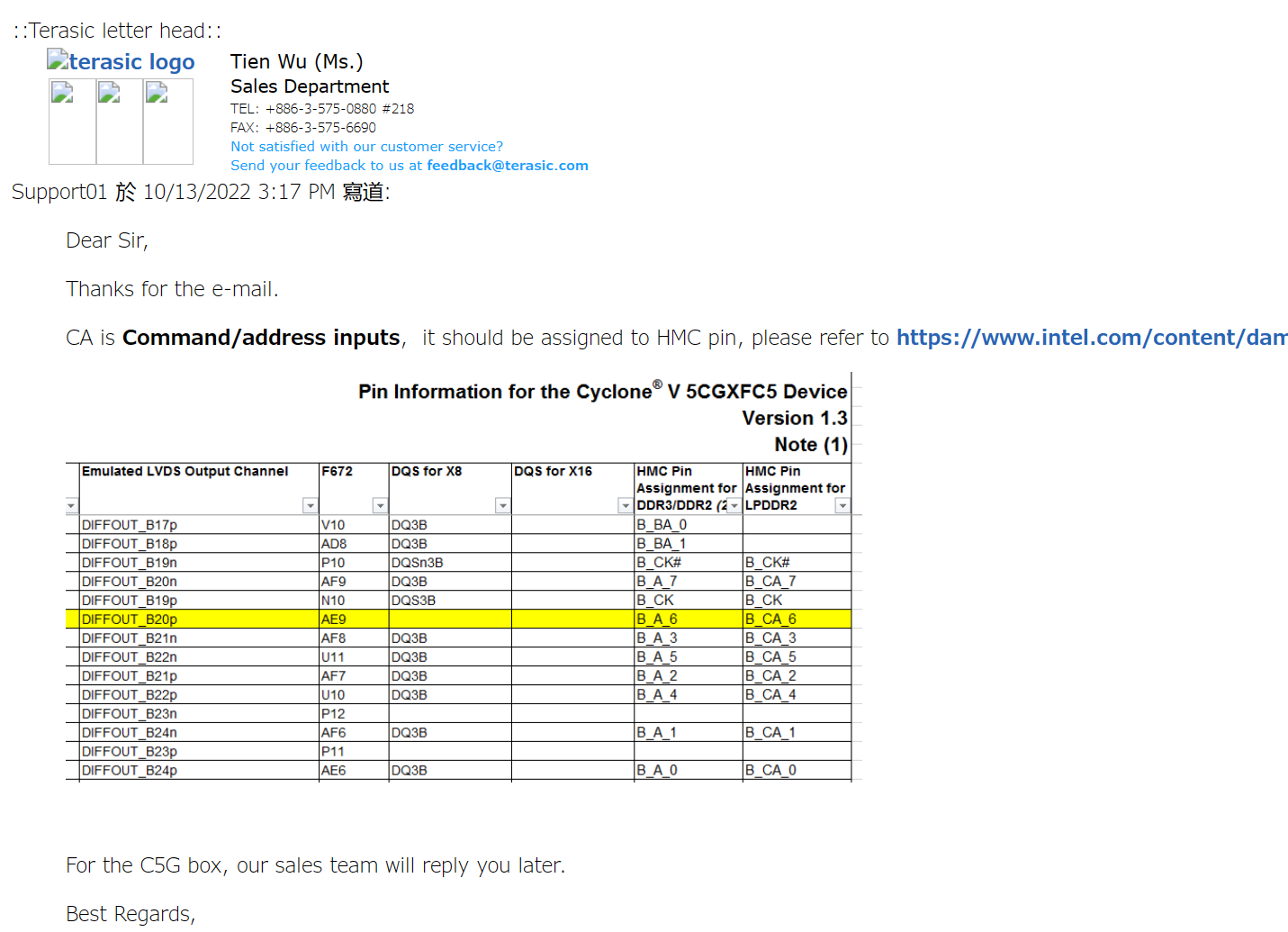
I understand that to use the memory I have to connect it using the information supplied with the board. This is what I did when I started a project to use the memory. I include a few screenshots; three show three pages of the Starter Kit user manual, listing all of the LPDDR2 pin locations. The other picture shows part of the Cyclone 5 GX pinout file from Intel. Both show that memory pin CA6 is connected to FPGA pin AE9.
This pin falls outside DQS group 3B, you can see this in the pinout file and the pin planner. THe pinoutfile also shows that the hard-memory controller (HMC) pin CA6 connects to FPGA pin AE9. However, this pin is not inside a DQS group while I think it is supposed to for the memory to work correctly through the hi-speed physical interface. Important to note is that pin AE8 is unconnected on the starter kit board. Pin AE8 is part of DQS group 3B. This suggests that I have to grab an iron and solder pins AE8 and AE9 together and keep AE9 in high-Z and use pin AE8 instead. Also, the CA pins of the memory seem not to be part of a DQS x16 group which means I would have to drive the command bus through 2 DQSx8 groups. That would be alright for this board.
However; I posted two different problems. This was the first problem. The second problem is separate from the kit and is research independent from the kit. The second problem is that fitter auto-place assignments do not match with the pin planner overview / legend. The Cyclone V manual says, if the user places only the DQS differential strobe (positive and negative pin), the fitter will then place all DQ pins associated with the DQS strobe into the same x8 or x16 group. For x16 groups this is not happening and DQ pins were placed randomly and now they are placed in the opposite bottom group; there are two DQS x16 groups at the bottom side.
This typical Cyclone 5 GX seems to support 2 HMC and each driving two separate command busses and 6 separate data channels, counting up to a 2-channel 24-bit memory controller per side, making this chip support 4-channel 24-bit DDR memory which looks like it is optimized for 24-bit DSP applications.
Thank you for your time.
P.S. I don't think something can be fixed and I think something is faulty, though not through Intel or Terasic doing.
- Mark as New
- Bookmark
- Subscribe
- Mute
- Subscribe to RSS Feed
- Permalink
- Report Inappropriate Content
Hello,
I don't think it's need to be placed in DQS group for this device.
Since it's hard memory controller, the placement must be follow on what has been stated in pinout file.
I will not say it's a faulty on this.
For the second problem, I'm not sure if there is any issue in Quartus regarding to the Fitter behavior.
Would you let me know about the Quartus version that has been used?
Regards,
Adzim
- Mark as New
- Bookmark
- Subscribe
- Mute
- Subscribe to RSS Feed
- Permalink
- Report Inappropriate Content
Hello Adzim,
I would like to let you know that I also examined the hard memory controller and the memory controller mega function. I ca tell the HMC and the Hi-PHY IP works together. The latter is the interface part to both the logic fabric but may also be driven by the hard memory controller.
The Quartus version I have been using is 20.1.1. Please look at the following file of a default Quartus install:
C:\intelFPGA_lite\20.1\quartus\libraries\megafunctions\xml_info\cyclonev_hmc_info.xml
This is an info file in XML format that tells what parameters and ports an atom has. This is the atom for the hard memory controller of a Cyclone V.
When you look at it, you will find a number of ports:
		<PORT NAME="afiaddr" TYPE="OUTPUT" WIDTH="20" DEFAULT_VALUE="0"/>
		<PORT NAME="aficke" TYPE="OUTPUT" WIDTH="2" DEFAULT_VALUE="0"/>
		<PORT NAME="aficsn" TYPE="OUTPUT" WIDTH="2" DEFAULT_VALUE="0"/>
		<PORT NAME="afidm" TYPE="OUTPUT" WIDTH="10" DEFAULT_VALUE="0"/>
		<PORT NAME="afiodt" TYPE="OUTPUT" WIDTH="2" DEFAULT_VALUE="0"/>
		<PORT NAME="afirdataen" TYPE="OUTPUT" WIDTH="5" DEFAULT_VALUE="0"/>
		<PORT NAME="afirdataenfull" TYPE="OUTPUT" WIDTH="5" DEFAULT_VALUE="0"/>
		<PORT NAME="afiwdata" TYPE="OUTPUT" WIDTH="80" DEFAULT_VALUE="0"/>
		<PORT NAME="afiwdatavalid" TYPE="OUTPUT" WIDTH="5" DEFAULT_VALUE="0"/>
The port names shown here connect directly to the corresponding atom parts of the hi-phy interface that you can find in my attached project RTL viewer. Pin "afiaddr" is the unpacked CA bus (20 lines) that go to the DDRIO units of the DQS pins Please note that in the pinout file, the clock pin (CLK) connects to DQS3B strobe pin; all other CA pins are part of DQ3B x8 group. Only CA6 is not in a group.
Hope this helps.
P.S. I have experience with being ssabotaged / having false information. This is done by a high-stakes third party and not by Intel. I do not say Intel provides false information or sabotages customers. I do not hold respondible Intel.
- Mark as New
- Bookmark
- Subscribe
- Mute
- Subscribe to RSS Feed
- Permalink
- Report Inappropriate Content
Hello,
There is no problem for Address/Command group to place outside of the DQS group.
DQS group is restricted to DQ, DM/DBI and DQS pins only.
Regards,
Adzim
- Mark as New
- Bookmark
- Subscribe
- Mute
- Subscribe to RSS Feed
- Permalink
- Report Inappropriate Content
Hello,
I will accept your answer for now; I do not want to get into a fight with Intel over this.
However, I will let you know that you may look for the "ADDCMD" clock source for the cyclonev_clock_phase_select atom in the generated sources when you instantiate the memorycontroller IP mega function. That's where you will find that the cyclonev_hmc atom connects to the ddout atom of a pad which is clocked by the clock wire that is connected to the DQS3B clock pin. Also, the OCT and DLL component are still required; I remember these are instantiated inside the megafunction source as well.
Anyways, you may close the thread and I thank you for your time.
- Mark as New
- Bookmark
- Subscribe
- Mute
- Subscribe to RSS Feed
- Permalink
- Report Inappropriate Content
Hello once more,
I would like to leave a final comment on this thread. I understand that the Cyclone V with the given pinout works fine when using the hmc (hard memory controller) and that it is correct to use pin AE9 for memory pin CA6. So, I'll take satisfaction with the fact that the board would probably work just fine there. However, my issue was with using the DQ x16 groups for the purpose of implementing a custom memory controller. According to the application note "High speed memory interfaces" custom memory controllers are possible and are allowed to be implemented; at least that is the suggestion. I understand however, that this way of implementing a memory controller would not work on the Cyclone V starter kit because it would require a different pinout.
Nonetheless, when it comes to the fitter's choice of placing DQ x16 pins with the user placed DQS x16 pin, the pin placement still does not match the legend; the pins are not placed in what the legend says is the DQS x16 group. I have tried different Cyclone types; for instance the smalled FBGA E-series model and noted that here also, the fitter autoplacement of DQ pins does not match what the legend says.
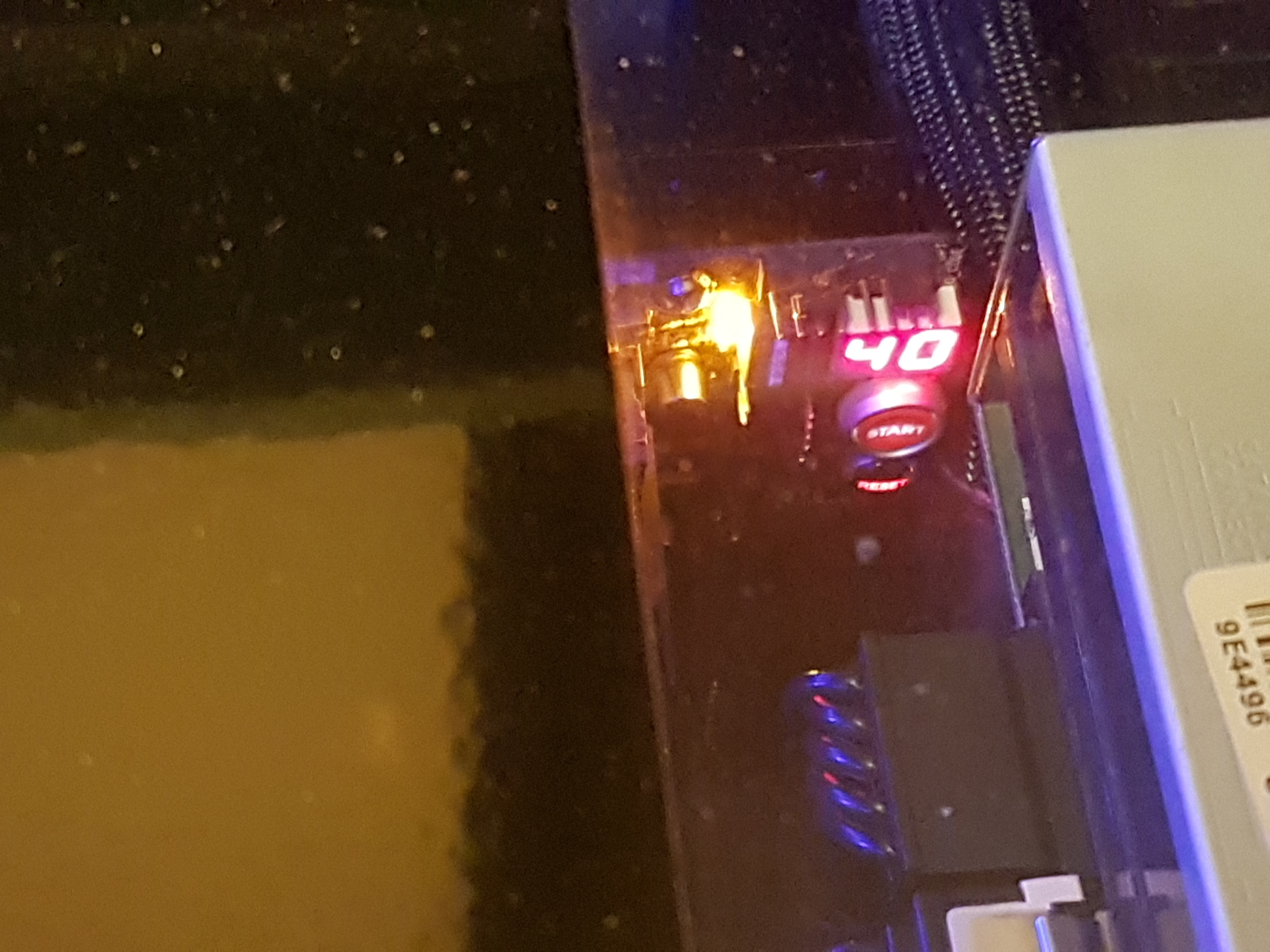
And now, a final note. I have been sporting an Intel CPU, an 5960X since 2015 along with an Asus rampage V extreme motherboard. Performance wise still very capable and usable. It has this BIOS debug code display on board that I can view any time by looking through the PC box top window. Since about 2019 and on, the BIOS code shows 40 hex. while it is supposed to show AA hex. Everything works fine overall. When I shut down windows, the BIOS debug code changes. It is briefly notable before system power shutdown. It then says 04 hex. It happens as part of the Windows shutdown. I know no OS would write codes shutdown. Also I've re-installed Windows 10 a good number of times. The problem persists. Now I know you are not a PC support forum but you might find it noteworthy that the startup and shutdown BIOS code basically says...:
40 04. Yes, that's your first CPU you made.
- Subscribe to RSS Feed
- Mark Topic as New
- Mark Topic as Read
- Float this Topic for Current User
- Bookmark
- Subscribe
- Printer Friendly Page