- Mark as New
- Bookmark
- Subscribe
- Mute
- Subscribe to RSS Feed
- Permalink
- Report Inappropriate Content
Error (170143): Final fitting attempt was unsuccessful
Info (170138): Failed to route the following 2 signal(s)
Info (170139): Signal "tic:tic4|WideOr4~0"
Info (170139): Signal "tic:tic6|stop_delt_flag[1]"
Info (170140): Cannot fit design in device -- following 2 routing resource(s) needed by more than one signal during the last fitting attempt
Info (170141): Routing resource LAB Input (X14_Y8, I16)
Info (170141): Routing resource LAB Input (X14_Y10, I35)
Error (11802): Can't fit design in device. Modify your design to reduce resources, or choose a larger device. The Intel FPGA Knowledge Database contains many articles with specific details on how to resolve this error. Visit the Knowledge Database at https://www.altera.com/support/support-resources/knowledge-base/search.html and search for this specific error message number.
Error: Quartus Prime Fitter was unsuccessful. 2 errors, 70 warnings
Error: Peak virtual memory: 7414 megabytes
Error: Processing ended: Tue Mar 05 17:25:28 2024
Error: Elapsed time: 00:02:21
Error: Total CPU time (on all processors): 00:04:13
I am working on someone else's circuit board and cannot modify the pins or replace the chip。
Link Copied
- Mark as New
- Bookmark
- Subscribe
- Mute
- Subscribe to RSS Feed
- Permalink
- Report Inappropriate Content
Without seeing the code, it's not really possible to understand what is happening here. Also would be helpful to know what device you're targeting and what version of Quartus you're using. Basically need more info here.
- Mark as New
- Bookmark
- Subscribe
- Mute
- Subscribe to RSS Feed
- Permalink
- Report Inappropriate Content
Yes more information needed to figure out this issue. You may check the resource report to see why and what resources are exhausted.
- Mark as New
- Bookmark
- Subscribe
- Mute
- Subscribe to RSS Feed
- Permalink
- Report Inappropriate Content
Thank you for your reply. The file attached below is the code for the tic module. The purpose of this module is to accurately measure the time interval between the arrivals of two levels. Could you advise on how to optimize the code to improve timing and layout? The rest of the project files are proprietary to the company and cannot be released.
- Mark as New
- Bookmark
- Subscribe
- Mute
- Subscribe to RSS Feed
- Permalink
- Report Inappropriate Content
- Mark as New
- Bookmark
- Subscribe
- Mute
- Subscribe to RSS Feed
- Permalink
- Report Inappropriate Content
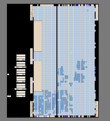
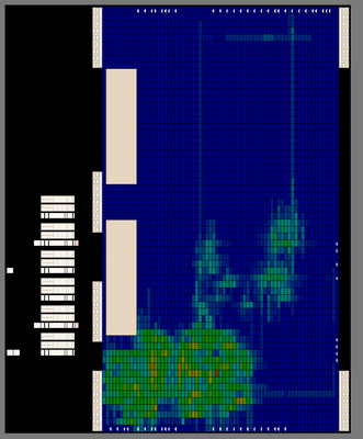
"I don't know if this is related. I observed in the chip planner that all the logic layout is concentrated in the bottom left corner, leaving many resources unused, yet my pins are distributed on three sides. Congestion occurs even when there are still many resources remaining."
The image below is a report of routing utilization.
The blue areas in the image below represent the pins I have actually allocated.

- Mark as New
- Bookmark
- Subscribe
- Mute
- Subscribe to RSS Feed
- Permalink
- Report Inappropriate Content
I found that changing the initial placement seed seems to solve the problem. However, I still want to know how to avoid this issue by modifying the code?
- Mark as New
- Bookmark
- Subscribe
- Mute
- Subscribe to RSS Feed
- Permalink
- Report Inappropriate Content
What device is this and what speed are you trying to run at? Do you have a .sdc and are you meeting all timing requirements?
- Mark as New
- Bookmark
- Subscribe
- Mute
- Subscribe to RSS Feed
- Permalink
- Report Inappropriate Content
Thank you for your reply.
I am using the Cyclone V 5CGXFC5C6F23C6. The code for the SDC file is in the attached file.Although I named it as a 500M clock, I actually reduced the frequency to 400M in practice. This can be seen in the SDC file.
By changing the seed to a specific value, after the compilation passes, there are timing violations.
The setup time violation is about 0.6ns.
- Mark as New
- Bookmark
- Subscribe
- Mute
- Subscribe to RSS Feed
- Permalink
- Report Inappropriate Content
You can check whether the clock frequency in your design is relatively high, and whether there are signals with large fan-out and large data bit widths. These factors can lead to concentrated routing
- Mark as New
- Bookmark
- Subscribe
- Mute
- Subscribe to RSS Feed
- Permalink
- Report Inappropriate Content
Thank you for your reply.
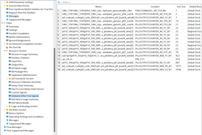
My data has a maximum bit width of 40 bits. I am not sure if this is considered wide data. Moreover, from the fitter report, there are no large fan-outs except for the clock signal. If there is a way to view all fan-out situations from other locations, please let me know.

- Mark as New
- Bookmark
- Subscribe
- Mute
- Subscribe to RSS Feed
- Permalink
- Report Inappropriate Content
You may try to disable the "optimize timing" setting in Advanced Setting (Fitter) and see if it will help the routing process.
- Mark as New
- Bookmark
- Subscribe
- Mute
- Subscribe to RSS Feed
- Permalink
- Report Inappropriate Content
Hi there, is there any updates on this?
- Mark as New
- Bookmark
- Subscribe
- Mute
- Subscribe to RSS Feed
- Permalink
- Report Inappropriate Content
Thank you for your reply. I tried your suggestion, and it indeed helped with the layout and routing, making some previously unsuccessful routings successful. However, it worsened the timing. This might be an area where a trade-off is necessary.
- Mark as New
- Bookmark
- Subscribe
- Mute
- Subscribe to RSS Feed
- Permalink
- Report Inappropriate Content
Yes, indeed. Additionally, 400M is somewhat high for Cyclone V, making it challenging to meet both layout and timing requirements simultaneously
- Mark as New
- Bookmark
- Subscribe
- Mute
- Subscribe to RSS Feed
- Permalink
- Report Inappropriate Content
Please login to ‘https://supporttickets.intel.com’, view details of the desire request, and post a feed/response within the next 15 days to allow me to continue to support you. After 15 days, this thread will be transitioned to community support. The community users will be able to help you on your follow-up questions.
- Subscribe to RSS Feed
- Mark Topic as New
- Mark Topic as Read
- Float this Topic for Current User
- Bookmark
- Subscribe
- Printer Friendly Page
