- Mark as New
- Bookmark
- Subscribe
- Mute
- Subscribe to RSS Feed
- Permalink
- Report Inappropriate Content
Hi;
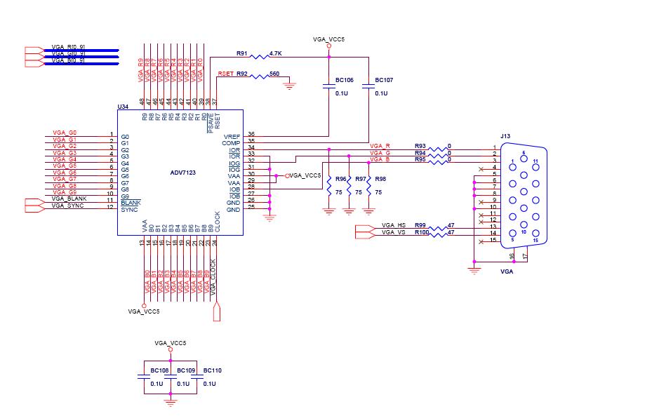
I student "Trainee" work with the kit of development-DE2- developed by TERASIC. I found the plan of interface between the DAC " ADV7123 " and the connector VGA. " Please look at the attached file ". I want to know: 1/ why did they connect the hsyn and vsyn with the resistance? And why is the value of the resistor is 47 ohms? 3/ the same question for these resistors ( R93, R94, R95, R96, R97, R98) ??? 2/ why did they use these 3 condensers BC108,BC109 and BC110 ? and why is the value of condenser is 0.1us?? Thanks:) Best regards; ALRIFAI HussamLink Copied
2 Replies
- Mark as New
- Bookmark
- Subscribe
- Mute
- Subscribe to RSS Feed
- Permalink
- Report Inappropriate Content
- Mark as New
- Bookmark
- Subscribe
- Mute
- Subscribe to RSS Feed
- Permalink
- Report Inappropriate Content
1/ why did they connect the hsyn and vsyn with the resistance? And why is the value of the resistor is 47 ohms?
The resistors seem to be used as current limiting resistors in this case. The author of the circuit diagram might be worried about the current flowing out of the ADV7123 and into the connector. I have used this device without the resistors and have not had a problem. They could also just be series termination resistors with the value(s) of 47 ohms determined by a package like Hyperlinx to maximize the signal integrity. An alternative (cheaper) way of determining this value is to use the IBIS file of the ADV7123 device and whatever you will plug into at the other end. 3/ the same question for these resistors ( R93, R94, R95, R96, R97, R98) ??? R93, R94, R95 are there for the same reason although in this case the author of the diagram plans to use these as part of plan B! Hence the 0 ohm resistors. R96, R97, R98 - VGA R,G,B signals are typically high frequency signals transferred from source to load via a transmission line. The impedances at each end of the line must be matched to the transmission line's characteristics hence the use of R96, R97 and R98 as impedance matching resistors. 2/ why did they use these 3 condensers BC108,BC109 and BC110 ? and why is the value of condenser is 0.1us?? According to the schematic the ADV7123 device has three voltage supply pins - 13,29,30 - which need a relatively clean and stable power supply input voltage with as little a ripple voltage as possible. A 0.1u capacitor connected as close as possible to each of these pins is a typical way of attaining this. I hope this helps
Reply
Topic Options
- Subscribe to RSS Feed
- Mark Topic as New
- Mark Topic as Read
- Float this Topic for Current User
- Bookmark
- Subscribe
- Printer Friendly Page