- Mark as New
- Bookmark
- Subscribe
- Mute
- Subscribe to RSS Feed
- Permalink
- Report Inappropriate Content
Previous (and presumed dead) discussions:
https://community.intel.com/t5/Programmable-Devices/Intel-Agilex-FHT-FGT-lane-swapping/m-p/1453468
https://community.intel.com/t5/Intel-Quartus-Prime-Software/Aglix-F-tile-P-amp-R-error/m-p/1456868
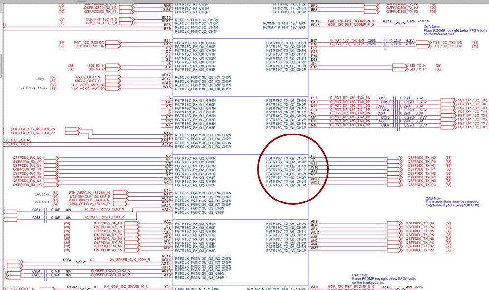
Been trying to drive signals out the QSFP-DD cages on my Agilex 027 SoC evm. Quartus is complaining about the pin assignments when I configure a quad of outputs (one instance, 4 lanes) in Platform Designer. The pins in question, from the SoC evm schematic:
I turned on all 16 FGT transceivers in an F-Tile to see where the compiler wanted to place them. Here's the breakdown of mappings from core signals to I/O pins:
All 16 FGT transceivers assigned.  Pins selected by Quartus (no constraints in .qsf)
qsfpdd0_tx0	Output		PIN_AD7		 Quad3[0]
qsfpdd0_tx1	Output		PIN_AG10	 Quad3[1]
qsfpdd0_tx2	Output		PIN_AH7		 Quad3[2]
qsfpdd0_tx3	Output		PIN_AM7		 Quad3[3]
hssi4p	Output			PIN_AC10	Quad2[3]
hssi5p	Output			PIN_Y7		Quad2[2]
hssi6p	Output			PIN_W10		Quad2[1]
hssi7p	Output			PIN_T7		Quad2[0]
hssi8p	Output			PIN_R10		 Quad1[3]
hssi9p	Output			PIN_M7		 Quad1[2]
hssi10p	Output			PIN_L10		 Quad1[1]
hssi11p	Output			PIN_G10		 Quad1[0]
hssi12p	Output			PIN_H13		Quad0[3]
hssi13p	Output			PIN_D13		Quad0[2]
hssi14p	Output			PIN_G16		Quad0[1]
hssi15p	Output			PIN_C16		Quad0[0]

Note that bits out[3:0] map to Quad3[3:0] but
out[7:4] map to Quad2[0:3] - bus twist
out[11:8] map to Quad1[0:3] - bus twist
out[15:12] map to Quad0[0:3] - bus twist
Appears there's bus twist at the Tile level, then again at the Quad level. So, "bus twist"? Wazzat?
Typically, it's a head-butting of big-endian and little-endian perspectives. Simple verilog example that assigns one 8-bit bus to another:
Abus[7:0] <= Bbus[0:7];
No big deal, right? The values of Bbus got assigned to Abus. What's really happening:
Abus[7] <= Bbus[0];
Abus[6] <= Bbus[1];
Abus[5] <= Bbus[2];
Abus[4] <= Bbus[3];
Abus[3] <= Bbus[4];
Abus[2] <= Bbus[5];
Abus[1] <= Bbus[6];
Abus[0] <= Bbus[7];
I'm running Quartus Pro 23.3, but this was observed in 23.1 and 22.3. If I try to map my output qsfp_dd[0] to pin T7 (which is FGTR13C_TX_Q2_CH0p) I will get an error saying there's no resource available or that the signal must be mapped to a different set of internally-named pins with a [3] suffix. If I twist my bus outputs such that out[3] is mapped to FGT_CH0p, it connects just fine. Notably, I did NOT have this issue with an Agilex AGF014 eval board that I was using previously. That one used E-Tiles, so this might be specific to the F-Tile implementation.
This type of problem is common for bussed signals (vectors) that cross a hierarchy boundary and the top-level and bottom-level declarations have opposite endian-ness.
I'm just going to patch around this issue with a macro-reassignment at my top-level that spackles-over the twist. Would be nice is Altera could fix the source issue in Quartus.
Link Copied
- Mark as New
- Bookmark
- Subscribe
- Mute
- Subscribe to RSS Feed
- Permalink
- Report Inappropriate Content
Hi,
Can you please share your project in which you observe the bus reversal.
Thank you,
Kshitij Goel
- Mark as New
- Bookmark
- Subscribe
- Mute
- Subscribe to RSS Feed
- Permalink
- Report Inappropriate Content
Ah, the hotkey <F3> canned response. But I'll provide more info because you asked me to, all sweet like.
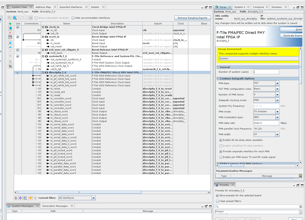
The design is about as brain-dead as it gets - define a TX Simplex output in Platform Designer, then blast static pattern data out using the provided clocks (which are derivative from the 156.25 FGT reference oscillator connected to this F-Tile externally.)
At the top level, instantiate the Platform Designer primitive, then map those HSSI signals to the attendant pins (use Pin Planner if you're a masochist, or just edit the ASCII text in the .qsf file directly.)
#
# Socket 0
set_location_assignment PIN_R14 -to clk_13c_fgt_refclk4_p
set_instance_assignment -name IO_STANDARD CML -to clk_13c_fgt_refclk4_p -entity top
set_location_assignment PIN_AC10 -to qsfpdd0_tx3
set_location_assignment PIN_Y7 -to qsfpdd0_tx2
set_location_assignment PIN_W10 -to qsfpdd0_tx1
set_location_assignment PIN_T7 -to qsfpdd0_tx0
You'll note that these pin assignments match those highlighted in the original post. Smack the "compile" button and let 'er rip!
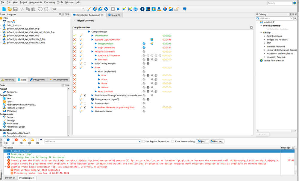
The system will fault when trying to place the HSSI signals on pins:
Here's the error transcript with some high-tech "word wrap" enabled:
Error(22144): Cannot place the block u0|directphy_f_0|directphy_f_0|dphy_hip_inst|persystem[0].perxcvr[0].fgt.tx_ux.x_bb_f_ux_tx at location fgt_q2_ch0_tx because the connected cell u0|directphy_f_0|directphy_f_0|dphy_hip_inst|persystem[0].perehip_tx[0].tx_ehip.x_bb_f_ehip_tx|bb_f_ehip_tx_xcvr25g0 can only be placed in location(s) bb_f_ehip_tx_xcvr25g[0], bb_f_ehip_tx_xcvr25g[4], bb_f_ehip_tx_xcvr25g[8], bb_f_ehip_tx_xcvr25g[12], bb_f_ehip_tx_xcvr25g[16], bb_f_ehip_tx_xcvr25g[20].

Error: Design cannot be programmed onto available F-Tiles because given location constraints are conflicting, or because the design requires more resources compared to what is available on current device
Amusingly, it's complaining that output[0] cannot be placed at location "ch[0]" because it can only be placed at locations [0], [4], [8], [12], [16], and [20]. If you edit the pin assignments to map output[0] -> ch[3] etc. (i.e. introduce the bus twist) it'll compile just fine. The top-level verilog maintains subordinate-entity continuity throughout - parallel data [0] maps to PD entity input [0], etc - but none of that really matters. The problem is the HSSI serial output connection to the physical pin.
.directphy_f_0_tx_serial_data_xcvr0_tx_serial_data     (qsfpdd0_tx0),     //  output,   width = 1,   		.directphy_f_0_tx_serial_data_xcvr1_tx_serial_data     (qsfpdd0_tx1),     //  output,   width = 1,
.directphy_f_0_tx_serial_data_xcvr2_tx_serial_data     (qsfpdd0_tx2),     //  output,   width = 1,
.directphy_f_0_tx_serial_data_xcvr3_tx_serial_data     (qsfpdd0_tx3),     //  output,   width = 1,
Top-level verilog and .qsf files are attached.
I look forward to being scraped-off to "community support" (hotkey <F5>) in short order!
- Mark as New
- Bookmark
- Subscribe
- Mute
- Subscribe to RSS Feed
- Permalink
- Report Inappropriate Content
Hi,
In the shared zip files, IP files are missing. Please the QAR file.
Also, as you have mentioned you don't see this issue in Q23.3. Please confirm.
Thank you,
Kshitij Goel
- Mark as New
- Bookmark
- Subscribe
- Mute
- Subscribe to RSS Feed
- Permalink
- Report Inappropriate Content
>> Also, as you have mentioned you don't see this issue in Q23.3. Please confirm.
No, that's not what I said. The problem exists in Q23.3 for the AGI027 target device. I do *not* see the bus twist issue when I target the AGF014 device. Seems to be an "I-Series" versus "F-Series" target issue, likely because the F-Series device was equipped with E-Tiles.
I have provided you with more than enough information and supporting documentation for you to replicate this problem on your own. It's super easy ... barely an inconvenience. I'm not going to do your job for you, and I'm certainly not going to do so without monetary compensation. Normally I'd offer you a consulting rate ... but I don't think I'll do that this time.
Have a nice day.
- Mark as New
- Bookmark
- Subscribe
- Mute
- Subscribe to RSS Feed
- Permalink
- Report Inappropriate Content
Hi,
As we do not receive any response from you on the previous question that we have provided. Please login to ‘https://supporttickets.intel.com’, view details of the desire request, and post a response within the next 15 days to allow me to continue to support you. After 15 days, this thread will be transitioned to community support. The community users will be able to help you on your follow-up questions.
Thank you,
Kshitij Goel
- Mark as New
- Bookmark
- Subscribe
- Mute
- Subscribe to RSS Feed
- Permalink
- Report Inappropriate Content
I am getting similar errors for AGF027 board. Is this due to bus-twist? Is this a Quartus issue and will it get fixed? I am using Quartus 23.4.
- Subscribe to RSS Feed
- Mark Topic as New
- Mark Topic as Read
- Float this Topic for Current User
- Bookmark
- Subscribe
- Printer Friendly Page


