- Mark as New
- Bookmark
- Subscribe
- Mute
- Subscribe to RSS Feed
- Permalink
- Report Inappropriate Content
Hi!Everybody!
I am confused by the Allow Any Shift Register Size for Recongnition Option in the more settings of Compilation & Analysis settings. ------------------------------------------------------- The following is the resource code. module test(clk,shift,sr_in,sr_out); input clk,shift; input sr_in; output sr_out; reg [63:0]shift_reg; always @(posedge clk) begin if (shift==1'b1) shift_reg[63:1] <= shift_reg[62:0]; shift_reg[0] <= sr_in; end assign sr_out = shift_reg[63]; endmodule --------------------------------------------- As we all know,It's only a Signal-Bit Wide,64-Bit Shift Register.I am confused by that when I set the Allow Any Shift Register Size for Recongnition Option to "ON", the using resource make me very surprise,this is the printscreen: http://images.cnblogs.com/cnblogs_com/tdyizhen1314/257630/r_2on.png However, when I set the Allow Any Shift Register Size for Recongnition Option to "OFF", the following is the printscreen of Compilation report: http://images.cnblogs.com/cnblogs_com/tdyizhen1314/257630/r_2off.png I think,when I set the Allow Any Shift Register Size for Recongnition Option to "ON", Quartus II should use registers to implement it, not combinational logic or Memory bits, and when I set the Option to "OFF", Either registers or combinational logic is possible , So Can you tell me the reason between the two compilation report, thanks!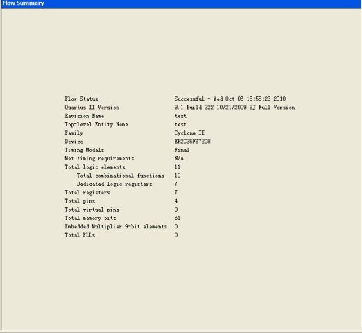
Link Copied
6 Replies
- Mark as New
- Bookmark
- Subscribe
- Mute
- Subscribe to RSS Feed
- Permalink
- Report Inappropriate Content
Does anyone know? I need help! many thanks!
- Mark as New
- Bookmark
- Subscribe
- Mute
- Subscribe to RSS Feed
- Permalink
- Report Inappropriate Content
I would use RTL viewer to see how the circuit was implemented after each compile. That would shed some light on what this option is doing.
- Mark as New
- Bookmark
- Subscribe
- Mute
- Subscribe to RSS Feed
- Permalink
- Report Inappropriate Content
Thanks for your reply,Nails!
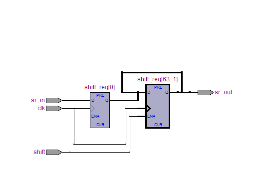
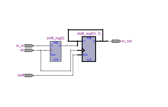
I did that before, there is no difference between the two sitution in RTL, but when having a look about the technology map viewer seriously, I am aware of the circuit implemented by the option(Allow any shift register size for recongnition ON) is more complex than OFF. and I am studying from it now.- Mark as New
- Bookmark
- Subscribe
- Mute
- Subscribe to RSS Feed
- Permalink
- Report Inappropriate Content
By the looks of it, one method uses the on-chip memory for the 64 bit register, and the other implements it in dedicated registers.
If the schematic is truly identical, perhaps you are only looking at the highest level schematic, and need to right-click on the memory block/shift_reg register (or some other block) in the schematic to go down one heirarchy to reveal how that is implemented to see the differences.- Mark as New
- Bookmark
- Subscribe
- Mute
- Subscribe to RSS Feed
- Permalink
- Report Inappropriate Content
--- Quote Start --- I think,when I set the Allow Any Shift Register Size for Recongnition Option to "ON", Quartus II should use registers to implement it, not combinational logic or Memory bits, and when I set the Option to "OFF", Either registers or combinational logic is possible --- Quote End --- I think you're partly misunderstanding the option. shift register recognition implies putting shift registers to internal RAM, no recognition to registers. Combinational logic isn't an option for shift registers in any case. As you can see from the register and RAM resource utilization in the report, Quartus is just doing this, you don't need to review the gate level net lists.
- Mark as New
- Bookmark
- Subscribe
- Mute
- Subscribe to RSS Feed
- Permalink
- Report Inappropriate Content
--- Quote Start --- By the looks of it, one method uses the on-chip memory for the 64 bit register, and the other implements it in dedicated registers. If the schematic is truly identical, perhaps you are only looking at the highest level schematic, and need to right-click on the memory block/shift_reg register (or some other block) in the schematic to go down one heirarchy to reveal how that is implemented to see the differences. --- Quote End --- Hi! Nails! You said"If the schematic is truly identical, perhaps you are only looking at the highest level schematic, and need to right-click on the memory block/shift_reg register (or some other block) in the schematic to go down one heirarchy to reveal how that is implemented to see the differences." However,there is no difference between the two RTL schematics.e.g. This is the RTL screenprint when the option is set to ON. http://images.cnblogs.com/cnblogs_com/tdyizhen1314/257630/r_on_rtl1.png and when the option is set to OFF. http://images.cnblogs.com/cnblogs_com/tdyizhen1314/257630/r_off_rtl1.png I tried,and I knew this was the highest level schematic,but It could't go down again by right-click. In fact, FvM had told the differences. I was misunderstanding the option before.Thanks for your reply again!
Reply
Topic Options
- Subscribe to RSS Feed
- Mark Topic as New
- Mark Topic as Read
- Float this Topic for Current User
- Bookmark
- Subscribe
- Printer Friendly Page