- Mark as New
- Bookmark
- Subscribe
- Mute
- Subscribe to RSS Feed
- Permalink
- Report Inappropriate Content
Greetings,
I'm trying to implement the following design on a Cyclone II DE2:
![20181015_234606[1].jpg](/t5/image/serverpage/image-id/203iBAABCA2043DAE1F1/image-size/large?v=v2&px=999&whitelist-exif-data=Orientation%2CResolution%2COriginalDefaultFinalSize%2CCopyright "20181015_234606[1].jpg")
It is a cell of a special type of a PUF (physically unclonable function) called the TSRAM PUF, where it consists of cross-coupled pairs of tristate inverters. The inputs to the system are the enable signals, and the single output to the signal is the logic level that settles at the lower_response node (the upper_response node can also be taken as the output instead).
So I started out by designing a single tristate inverter like so:

And then I created a symbol out of the it, before using it to create the complete design:

There are many criteria that has to be satisfied in order for this design to work (I'll post the others as separate questions), one of them is that the circuit has to be physically symmetric, that is, the delay from each input/output of the tristate inverters to its facing node (lower or upper response) must be equal, and in order to do that, I have to be able to work with the individual tristate inverters in the chip planner, however, when I compile, the compiler "washes away" my design and leaves me with this:

My dilemma is that how can I force the compiler to "pass-through" my tristate inverters to the chip planner as they are without any optimization or change?
Any help or reference is highly appreciated.
If there is any additional information required, then please let me know.
Thank you all in advance,
My best regards.
Link Copied
- Mark as New
- Bookmark
- Subscribe
- Mute
- Subscribe to RSS Feed
- Permalink
- Report Inappropriate Content
Are you able to capture the technologies map viewer for tristate inverter block and overview of the design?
- Mark as New
- Bookmark
- Subscribe
- Mute
- Subscribe to RSS Feed
- Permalink
- Report Inappropriate Content
Yes, below is the tech. map viewer for the tristate inverter:

And here is the one for the overall design:

Additionally, here is the one for the tristate inverter instance (the green blocks above):

- Mark as New
- Bookmark
- Subscribe
- Mute
- Subscribe to RSS Feed
- Permalink
- Report Inappropriate Content
In FPGA architecture, there is no tristate primitive component in the core, specifically in LE block. Look at Cyclone II LE structure https://www.intel.com/content/dam/www/programmable/us/en/pdfs/literature/hb/cyc2/cyc2_cii5v1.pdf, Figure 2-3 
- Mark as New
- Bookmark
- Subscribe
- Mute
- Subscribe to RSS Feed
- Permalink
- Report Inappropriate Content
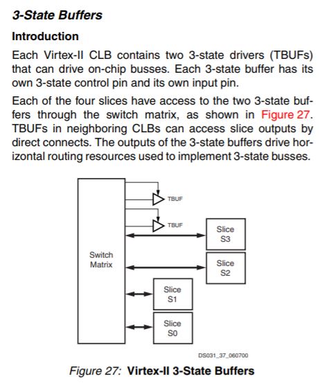
Is it possible to implement the design on any Altera FPGA other than the Cyclone II?
What about Xilinx FPGAs? Because I have a paper that implemented the same design on a Xilinx Virtex II (even though I didn't find any tristate support in its CLBs), a snippet of the paper is shown below:
![20180921_161028[1].jpg](/t5/image/serverpage/image-id/131iCE964327AA98B3B2/image-size/large?v=v2&px=999&whitelist-exif-data=Orientation%2CResolution%2COriginalDefaultFinalSize%2CCopyright "20180921_161028[1].jpg")
- Mark as New
- Bookmark
- Subscribe
- Mute
- Subscribe to RSS Feed
- Permalink
- Report Inappropriate Content
What I understand is all of Intel FPGAs do not have any tristate built either in ALM or LE primitive block. Checked on the Virtex II device datasheet, I believe it have it in their CLB.
- Mark as New
- Bookmark
- Subscribe
- Mute
- Subscribe to RSS Feed
- Permalink
- Report Inappropriate Content
May I ask you to point out exactly where you found the tristate component in the Xilinx datasheet:

Your help is highly appreciated.
- Mark as New
- Bookmark
- Subscribe
- Mute
- Subscribe to RSS Feed
- Permalink
- Report Inappropriate Content
- Subscribe to RSS Feed
- Mark Topic as New
- Mark Topic as Read
- Float this Topic for Current User
- Bookmark
- Subscribe
- Printer Friendly Page