- Mark as New
- Bookmark
- Subscribe
- Mute
- Subscribe to RSS Feed
- Permalink
- Report Inappropriate Content
Hi every one
I had designed a Combinational circuit in Quartus II 13.0 but it was not optimized as the number of input variables were so many I couldn't simplify it using Karnaugh Maps ,so I decided to draw whole truth table on the schematic environment with out pre-simplification, as I searched on the net I found out that Quartus does the simplification by it self after compilation. so after the compile I checked Netlist Viewers/technology map viewer(post filtering),I found the optimized circuit there ,I wonder if I can export or copy it from there and use it in schematic environment, on the other hand is there a way to import whole the truth table to the Quartus so that it automatically optimizes and makes logics by it self ? I'd be glad for any sort of hint. thank you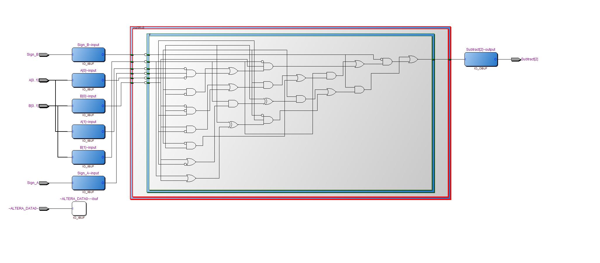
Link Copied
- Mark as New
- Bookmark
- Subscribe
- Mute
- Subscribe to RSS Feed
- Permalink
- Report Inappropriate Content
The Karnaugh Map has no sense on fpgas because it is oriented to AND-OR-NOT gates. In fpga you have 4-inputs look up tables. A way to implement a truth table when you can't describe with a logic expression or can't find a vhdl description, is an asynchoronous rom description in vhdl or veriflo and a lot of time to fill each row.
- Mark as New
- Bookmark
- Subscribe
- Mute
- Subscribe to RSS Feed
- Permalink
- Report Inappropriate Content
well I know what you mean but as a matter of fact in next step I have to Implement Transistor level of my digital circuit in ADS Software and simulated the whole Analog and digital parts together, so I need the optimized version of my digital circuit Individually.
could you plz explain more about "A way to implement a truth table when you can't describe with a logic expression or can't find a vhdl description, is an asynchoronous rom description in vhdl or veriflo and a lot of time to fill each row. "- Mark as New
- Bookmark
- Subscribe
- Mute
- Subscribe to RSS Feed
- Permalink
- Report Inappropriate Content
If I am given truth table to design in vhdl I will use case statement and expect the tool to do the rest old techniques.
e.g. A B C D E F out1 out2 out3 out4 0 0 0 0 0 0 1 0 1 1 ... case input is when "000000" => out <= "1011"; ... with a bit of concatenation- Mark as New
- Bookmark
- Subscribe
- Mute
- Subscribe to RSS Feed
- Permalink
- Report Inappropriate Content
yes thx dear but how about the Optimized circuit after compile? can you extract the VHDL code of the Optimized version of your code?
- Mark as New
- Bookmark
- Subscribe
- Mute
- Subscribe to RSS Feed
- Permalink
- Report Inappropriate Content
--- Quote Start --- yes thx dear but how about the Optimized circuit after compile? can you extract the VHDL code of the Optimized version of your code? --- Quote End --- The netlist is not vhdl and I don't know of conversion from netlist to schematic. However as mentioned a rom table will do in schematic. Your input will be the address. The contents will be the output e.g. for above example location 0 of rom should contain 1011 and soon.
- Mark as New
- Bookmark
- Subscribe
- Mute
- Subscribe to RSS Feed
- Permalink
- Report Inappropriate Content
actually as I said earlier I need schematic of the Optimized version to be extracted so that I can Import in to and other software, as you see the Image which I attached shows the optimized version but it's not editable or even I cant copy past it to Quartus Schematic Environment :(
- Mark as New
- Bookmark
- Subscribe
- Mute
- Subscribe to RSS Feed
- Permalink
- Report Inappropriate Content
Do you mean your software tool will not optimise the rom table?
option 1) so be it if it is implemented in rom (not logic) option 2) I know there were tools to optimise logic equations and tables but not sure if they are still around. and there might be ways of exporting from netlist...just a thought- Mark as New
- Bookmark
- Subscribe
- Mute
- Subscribe to RSS Feed
- Permalink
- Report Inappropriate Content
Let me ask my question this way
forget about FPGA and other things suppose I have Karnaugh Map of 6 Variable and I want Quartus to Minimize it and show me the result in a way that I can copy past it schematic environment. Is there a way? thx for you help dear- Mark as New
- Bookmark
- Subscribe
- Mute
- Subscribe to RSS Feed
- Permalink
- Report Inappropriate Content
I don't know if Altera would have thought of designing its quartus tool to support 3rd party pockets! But if you are after truth table reduction then make a search e.g. for "Karnaugh map minimisers"
- Mark as New
- Bookmark
- Subscribe
- Mute
- Subscribe to RSS Feed
- Permalink
- Report Inappropriate Content
well actually I searched for the Karnaugh Map Minimizers and I found some applications but I don't trust them as I tested one of them and saw the wrong result. I think the only thing I can do is to gave Truth table to Quartus using VHDL and see the Image result of optimized Karnaugh map and draw it Schematic Environment by myself.
- Mark as New
- Bookmark
- Subscribe
- Mute
- Subscribe to RSS Feed
- Permalink
- Report Inappropriate Content
We can't forget fpgas using Quartus. Probably ( 99,9% sure ) Quartus don't use Karnaugh maps. If you see in the tecnhology map viewer, the real implementation of a circuit, you see a multilevel implementation ( multi level LUT, NO multi level logic gate ), when Karnaugh map gives you a 2 level implementation. Quartus generates a good implementation for an Altera fpga. But there isn't the best circuit based on and-or-not gates. Use a software based on Quine-McKluskey method to get the kind of circuit you're looking for.
- Mark as New
- Bookmark
- Subscribe
- Mute
- Subscribe to RSS Feed
- Permalink
- Report Inappropriate Content
Thx dear bertulus for your reply
as I get from you statement you mean that it Quartus optimizes the circuit in the way that,it is best fit on the FPGA chip not the global Optimization done by Karnaugh map or even Quine-Mckluskey? well but as far as I know(watching some tutorial videos)I found out that it Optimizes the Circuit, and as a best of my knowledge there should be a pre-Optimization done by software. but as you mentioned I was looking for the software based on Quine-Mckluskey but I am not sure which software should I trust because they rarely guarantee the result, if you had used some sort of related software's I would be very thankful if you introduce me (I have 6 variables of inputs) YouTube link of tutorial videos "http://www.youtube.com/watch?v=qKv9LY_VRbc"- Mark as New
- Bookmark
- Subscribe
- Mute
- Subscribe to RSS Feed
- Permalink
- Report Inappropriate Content
also I should tell you that the photo I attached is Image of technology map viewer as you see it is Multi level logic gates and also here I saw an option that I saw karnaugh map of my circuit, so I don't think that you are right,
maybe on the Implementing to FPGA it acts as you said but I think before that it Minimizes the Circuit.- Subscribe to RSS Feed
- Mark Topic as New
- Mark Topic as Read
- Float this Topic for Current User
- Bookmark
- Subscribe
- Printer Friendly Page