- Mark as New
- Bookmark
- Subscribe
- Mute
- Subscribe to RSS Feed
- Permalink
- Report Inappropriate Content
Hello,
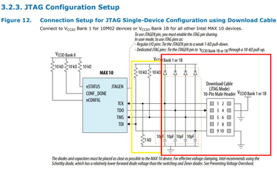
I am writing to you regarding the overshoot protection circuit (circled in red in the image).
These circuits are used for one-time use only, and I also have space constraints on my PCB.
I would like to ask if it is possible to make a separate sub-board for this circuit that can be connected during programming.
The GND of the two boards will be connected together,
and the voltage of the two boards will also be set to the same as VCCIO BANK1.
Is this feasible? If so, what are the things I need to pay attention to?
Thank you for your time and consideration.
Link Copied
- Mark as New
- Bookmark
- Subscribe
- Mute
- Subscribe to RSS Feed
- Permalink
- Report Inappropriate Content
I think, it's a matter of use case, in which environment programming will be performed.
- Mark as New
- Bookmark
- Subscribe
- Mute
- Subscribe to RSS Feed
- Permalink
- Report Inappropriate Content
Hi,
It is feasible to have the marked circuit on the separate board, provided the GND are connected and the VCCIO is sourced from the main board.
Regards
- Mark as New
- Bookmark
- Subscribe
- Mute
- Subscribe to RSS Feed
- Permalink
- Report Inappropriate Content
Hi,
As the query has been answered, I am setting the case to closure. However, it will still be open for the community members to comment on.
Regards
- Subscribe to RSS Feed
- Mark Topic as New
- Mark Topic as Read
- Float this Topic for Current User
- Bookmark
- Subscribe
- Printer Friendly Page
