- Mark as New
- Bookmark
- Subscribe
- Mute
- Subscribe to RSS Feed
- Permalink
- Report Inappropriate Content
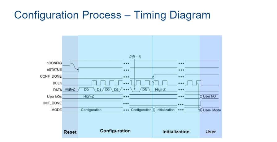
For the test I'm performing on the 10M08SCU169A7G, I'm trying to static bias the part, with no programming. Currently, I'm thinking the simplest way would be to test it in the reset mode. According to the MAX 10 Device Family Pin Connection Guidelines document, table 2, if I pull the nCONFIG pin low during user mode, the device will enter a reset state and tri-state all I/O pins. Can I keep the nCONFIG pin low at startup to keep the part from configuring? Also, when the part is in reset mode, are ALL I/O pins tri-stated? (including those that are dual-purpose pins with configuration function modes)
For the optional dual-purpose pins (i.e. IO/CRC_ERROR, IO/DEV_CLRn, and IO/DEV_OE), what state are they in while the device is in the reset state (IO pin mode or the configuration function mode)? Could you explain why the MAX 10 Device Family Pin Connection Guidelines document, table 2 states that these pins (as well as the TDO and TCK pins) are tri-state by default? What does that mean for my application?
The MAX 10 Device Family Pin Connection Guidelines document, table 7 mentions that the VCCIO[#] pins supply different power supplies, depending on the I/O standard assigned to each I/O bank. In a reset state, how does this effect the device's allowed voltage range?
Link Copied
- Mark as New
- Bookmark
- Subscribe
- Mute
- Subscribe to RSS Feed
- Permalink
- Report Inappropriate Content
Hi NBurt,
Can I keep the nCONFIG pin low at startup to keep the part from configuring?
Yes, you can pull nCONFIG low to keep MAX 10 from configure (in reset mode).
Are ALL I/O pins tri-stated?
Yes, all I/O pins (include dual-propose pins)
What state are they in while the device is in the reset state?
Tri-stated
What does that mean for my application?
For example, if MAX10 used to controls power to the entire system. Then, when reset state trigger, the IO pins tristate and the system shutdown.
In a reset state, how does this effect the device's allowed voltage range?
Only I/O pins are tri-stated when in reset state. Power pin function won’t affected in reset state.
Thanks.
- Mark as New
- Bookmark
- Subscribe
- Mute
- Subscribe to RSS Feed
- Permalink
- Report Inappropriate Content
Hi Wolfgang,
That's helpful. Thanks for the reply.
To clarify further, are there any non-power supply or GND pins that aren't tri-stated? Obviously, nConfig isn't, but are the JTAG pins tri-stated? Wouldn't you need them for the configuration (hence, they WOULDN'T be tri-stated)?
Concerning my last question, without configuration, how do I know which I/O standard is assigned to each bank? Will each bank have a different allowed voltage range?
Thanks,
Noah
- Mark as New
- Bookmark
- Subscribe
- Mute
- Subscribe to RSS Feed
- Permalink
- Report Inappropriate Content
Hi NBurt,
JTAG pins cannot perform as JTAG pins in user mode if you assign any of the JTAG pin as a
differential I/O pin. Thus, you must use the JTAG pins as dedicated pins and not as user I/O pins during JTAG programming
Concerning my last question, without configuration, how do I know which I/O standard is assigned to each bank?
You can go to Pin-Out Files for Intel FPGA Devices website page, and download you specific MAX 10 device. From here you will know which I/O standard is assigned to each bank.
https://www.intel.com/content/www/us/en/programmable/support/literature/lit-dp.html
Will each bank have a different allowed voltage range?
Yes, each bank will have different voltage range.
Thanks
- Subscribe to RSS Feed
- Mark Topic as New
- Mark Topic as Read
- Float this Topic for Current User
- Bookmark
- Subscribe
- Printer Friendly Page
