- Mark as New
- Bookmark
- Subscribe
- Mute
- Subscribe to RSS Feed
- Permalink
- Report Inappropriate Content
I am in the process of upgrading from QII 5.0 to QII 7.1 and I am facing some problems. My design is fairly large. One of the modules that I know is not working properly is a module that interfaces with an SRAM chip. I notice that when I compile the design in QII 7.1, I get the following new warning:
--- Quote Start --- Warning: Converting TRI node "SRAM_Control:SRAM_ARBITRATOR|bus_tri32uni:SRAM_TRISTATE_BUFFER|lpm_bustri:lpm_bustri_component|dout[31]" that feeds logic to an OR gate --- Quote End --- I do not get this warning when compileing in QII 5.0. I was wondering if anybody has any suggestions or if they have seen a similar warning. The SRAM_TRISTATE_BUFFER takes in data off of a PCI bus and outputs the data to the SRAM chip. The enable for the tristate buffer is a PCI_write signal. I don't know why it would try to convert it to an OR gate. Is there any way of disabling QuartusII from converting Tri state buffers? To fix the SRAM control logic I have also looked into timing requirements, but the timing is the same between QII 5.0 and QII 7.1. Thank you in advance.Link Copied
- Mark as New
- Bookmark
- Subscribe
- Mute
- Subscribe to RSS Feed
- Permalink
- Report Inappropriate Content
Is this a schematic? Does the tri directly feed a bidir pin(with a feedback path)? The only tri-states in the devices are in the IO cells and directly feed the pin, so unless your design exactly matches that, it has to convert it to logic(the conversion to logic works nicely for internal tri-state conversion, but since you're really doing a bidirectional signal, then you want to make sure this goes away.) Can you attach/describe how this is connected?
- Mark as New
- Bookmark
- Subscribe
- Mute
- Subscribe to RSS Feed
- Permalink
- Report Inappropriate Content
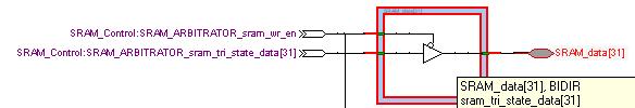
Hey, the tri state that is being converted is SRAM_TRISTATE_BUFFER. It was created by using the COMPONENT lpm_bustri form the MegaWizard. "sram_data" is bidirectional and it goes directly to the Data pins of the SRAM. "sram_tri_state_data" comes from the Data pins from the PCI bus. "not sram_wr_en" is just the PCI_write signal from the PCI bus. Is this the information you were looking for? Thanks.
PCI_RD_TRISTATE : bus_tri32uni port map ( data => sram_data, enabledt => PCI_RD_EN and not MODULE_EN, tridata => PCI_DATA ); SRAM_TRISTATE_BUFFER : bus_tri32uni port map ( data => sram_tri_state_data, enabledt => not sram_wr_en, tridata => sram_data );- Mark as New
- Bookmark
- Subscribe
- Mute
- Subscribe to RSS Feed
- Permalink
- Report Inappropriate Content
Yes, that looks correct(although I don't have the full picture). Are the pins declared as being type bidir? I've seen that be an issue before.
Can you look in the Technology Map Viewer or the Chip Editor and see if the tri-state is being used for those pins?- Mark as New
- Bookmark
- Subscribe
- Mute
- Subscribe to RSS Feed
- Permalink
- Report Inappropriate Content
- Mark as New
- Bookmark
- Subscribe
- Mute
- Subscribe to RSS Feed
- Permalink
- Report Inappropriate Content
The tri-state and enabel look correct. But there doesn't appear to be a feedback path on the bidir pin(i.e. when the tri-state is in the high-Z state, how does external logic drive back into the device?)
Also, looking at what you sent, why does sram_data feed another tri-state? Does it go off chip? You only need one tri-state per bidir, not two.- Subscribe to RSS Feed
- Mark Topic as New
- Mark Topic as Read
- Float this Topic for Current User
- Bookmark
- Subscribe
- Printer Friendly Page