- Mark as New
- Bookmark
- Subscribe
- Mute
- Subscribe to RSS Feed
- Permalink
- Report Inappropriate Content
Hi
We are using a NIOS2 processor and some VHDL code inside a Cyclone 2 240 pin package. Connected to the FPGA are 2 SRAM chips, EPCS16 and a couple of MLVDS transceivers, namely MLVD080 and MLVD205 from TI. This is the problem we are experiencing on our boards: If the system is configured to run directly from the input clock 32.768MHz on pin 92 then the system runs fine (NIOS and VHDL). But if we use the PLL with the VDDD and VDDA on pins 121 and 123 respectively the PLL loses lock with the frequency of the accesses to the MLVD080. The power supply for the PLL is as recommended by Altera (VDDA is filtered with a ferrite bead and a bank of capacitors from 2u2 down to 10nF, same for VDDD without the ferrite bead). The MLVD is blocked on its power supply with 100nF capacitors, also we tried adding bigger capacitors, 22uF, with no result. VDDD was also filtered the same way as VDDA, no effect. The board has 4 layers, with a power plane covering the whole board with cutouts for the 1.2V supply rail and a ground plane. Surrounding the PLL are data lines that go to and from the MLVD. We are contempt with the design running without the PLL but we would like to know what is behind this problem, since it may arise in the future the need for the PLL. Thank you in advance. :)Link Copied
11 Replies
- Mark as New
- Bookmark
- Subscribe
- Mute
- Subscribe to RSS Feed
- Permalink
- Report Inappropriate Content
My experience is, that PLL loose of lock with Cyclone II is mainly related to simultaneous switching outputs (SSO) generated ground bounce. I had a case, where it was impossible to operate a 32 bit data bus in a PQFP240 Cyclone II device, the issue was solved by configuring the bus to 16 bit, which was possible there, fortunately.
In the reported case, also the board layout and supply decoupling had been state of the art, actually no switching noise could be measured at the supply pins. From the circuit behaviour, it was obvious, that switching bus outputs caused loose of lock, but we couldn't reveal for sure, if the final reason was in ground bounce disturbing the clock input or the PLL analog supply. As we found a workaround, there was no high pressure to find a final solution. Although it wasn't verified, if single ended input clock contributes to the problem, I used a differential (LVDS) clock supply in several later design, hoping that it would be almost immune to ground bounce. New designs are also using Cyclone III, which is apparently less sensitive to analog supply interference for it's internal PLL voltage regulator. It also turned out, that PQFP240 is more susceptible to ground bounce than other packages due to large lead frame and long bond wires. Altera hasn't defined simultaneous switching output limits for single ended IO as e. g. for voltage referenced standards, but interferences may occur anyway, particularly with large PQFP package.- Mark as New
- Bookmark
- Subscribe
- Mute
- Subscribe to RSS Feed
- Permalink
- Report Inappropriate Content
Hi
"If the system is configured to run directly from the input clock 32.768MHz on pin 92 then the system runs fine (NIOS and VHDL)". how did you get the phase shift between the nios processor and the sram if u use the input clock? Thanks- Mark as New
- Bookmark
- Subscribe
- Mute
- Subscribe to RSS Feed
- Permalink
- Report Inappropriate Content
--- Quote Start --- Hi "If the system is configured to run directly from the input clock 32.768MHz on pin 92 then the system runs fine (NIOS and VHDL)". how did you get the phase shift between the nios processor and the sram if u use the input clock? Thanks --- Quote End --- We let the NIOS take care of that, just add the IDT71V416 SRAM component (avalon slave) and that's it, just take care when connecting pins for byte enable and current limits if they are close and no resistors present on the lines :) works every time so far :)
- Mark as New
- Bookmark
- Subscribe
- Mute
- Subscribe to RSS Feed
- Permalink
- Report Inappropriate Content
Hi Miilsod
Thanks for the reply.. I just have a couple of followup questions, because i am having the same issue with the SSRAM. 1) what clock is feading your ram...is it direct from your crystal, or does it go through the first? 2) can you elaborate further on the statement "just take care when connecting pins for byte enable and current limits if they are close and no resistors present on the lines http://www.alteraforum.com/images/smilies/smile.gif " Thanks http://www.alteraforum.com/images/smilies/smile.gif
- Mark as New
- Bookmark
- Subscribe
- Mute
- Subscribe to RSS Feed
- Permalink
- Report Inappropriate Content
--- Quote Start --- Hi Miilsod Thanks for the reply.. I just have a couple of followup questions, because i am having the same issue with the SSRAM. 1) what clock is feading your ram...is it direct from your crystal, or does it go through the first? 2) can you elaborate further on the statement "just take care when connecting pins for byte enable and current limits if they are close and no resistors present on the lines http://www.alteraforum.com/images/smilies/smile.gif " Thanks http://www.alteraforum.com/images/smilies/smile.gif --- Quote End --- 1. how can u feed clock through the ram first? :P You must mean the PLL? No, the clock feeds the design directly, inside the design the clock enters NIOS cpu and inside the cpu the design is as follows: - cpu - jtag uart - tri_state_bridge - sram and some other components. The same clock is used to drive peripheral VHDL logic in the same FPGA. 2. well you have to connect the correct BE to the address lines if you're using two SRAM chips otherwise strange things may happen (search for forum on NIOS printf problems, there are a couple of threads on that subject). As for current limits we found out that we had a bit of overshot or ground bounce, it manifested diferently on two identical boards, the solution was to limit drive current on sram pins. I hope i was clear enough, but you're still welcome with questions ;)
- Mark as New
- Bookmark
- Subscribe
- Mute
- Subscribe to RSS Feed
- Permalink
- Report Inappropriate Content
Hi Milosd..
Sorry for the confusion.. :( My question is, is pin 92 on your cyclone II the same point as the clock pins on your sram? If you can send me a diagram, or a brief schematic of your system, that will be very helpfull.. Thanks you very much for replying- Mark as New
- Bookmark
- Subscribe
- Mute
- Subscribe to RSS Feed
- Permalink
- Report Inappropriate Content
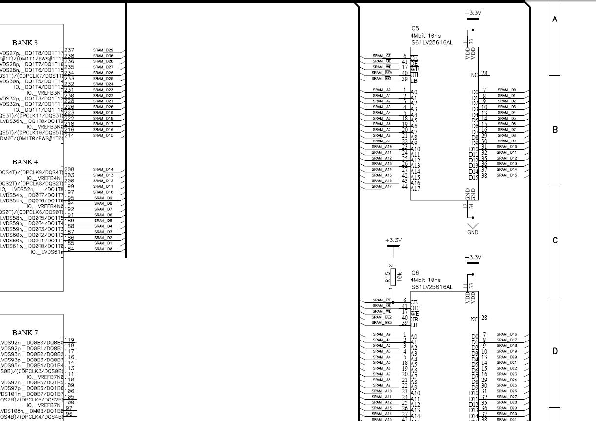
--- Quote Start --- Hi Milosd.. Sorry for the confusion.. :( My question is, is pin 92 on your cyclone II the same point as the clock pins on your sram? If you can send me a diagram, or a brief schematic of your system, that will be very helpfull.. Thanks you very much for replying --- Quote End --- Hmm I think you have a different RAM in mind... We are using Static RAM, meaning he doesn't require any clocks for operation since everything is tied to enable pins (write, read...) See the schematic attached.
- Mark as New
- Bookmark
- Subscribe
- Mute
- Subscribe to RSS Feed
- Permalink
- Report Inappropriate Content
Ahh..you r right..
I thought u were using a synchronous ram.. Thanks- Mark as New
- Bookmark
- Subscribe
- Mute
- Subscribe to RSS Feed
- Permalink
- Report Inappropriate Content
No prob :)
- Mark as New
- Bookmark
- Subscribe
- Mute
- Subscribe to RSS Feed
- Permalink
- Report Inappropriate Content
Hi Milosd..
Did u ever find a solution to your PLL problem? Thanks- Mark as New
- Bookmark
- Subscribe
- Mute
- Subscribe to RSS Feed
- Permalink
- Report Inappropriate Content
Well we have a board ready to be sent for production but since the cost for prototypes is a bit high we decided for now to stick with the current solution. Which means it'll rear its ugly head when we least expect to :)
Reply
Topic Options
- Subscribe to RSS Feed
- Mark Topic as New
- Mark Topic as Read
- Float this Topic for Current User
- Bookmark
- Subscribe
- Printer Friendly Page