- Mark as New
- Bookmark
- Subscribe
- Mute
- Subscribe to RSS Feed
- Permalink
- Report Inappropriate Content
I'm working on a schematic with a 10M25DAF256I7G.
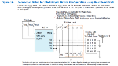
I'm going to power the FPGa with supply scheme as stated on Pin Connection Guide Line page 20: VCC: 1.2V VCCINT: 1.2V VCCD_PLL: 1.2V VCCA:2.5V VCCA_ADC:2.5V VCCIO:3.3V I have a problem to understand the JTAG pull-up voltage. As stated on Pin Connection Guide Line: "for configuration voltage of 2.5v, 3.0v or 3.3v, connect this pin through a 10kohm resistor to 2.5v (vccio bank 1 b) to prevent voltage overshoot..." But my VCCIO is 3.3V for all banks. Why it says 2.5V? Furthermore in the MAX10 Configuration User guide on page 3-3 the pull resistor are at VCCIO Bank 1B with clamp diode. So i think i can pull-up to 3.3V. My question is: If i use a configuration scheme as stated on page 20 of the Pin Connection Guide Line, how do i have to connect the jtag pull-up resistor for JTAG signals? Is it 2.5V or 3.3V with diode as stated in the Connection guide line? ThanksLink Copied
- Mark as New
- Bookmark
- Subscribe
- Mute
- Subscribe to RSS Feed
- Permalink
- Report Inappropriate Content
Yes, you can connect the pull-ups to 3.3V.
Refer to the 'max 10 fpga configuration user guide (https://www.altera.com/content/dam/altera-www/global/en_us/pdfs/literature/hb/max-10/ug_m10_config.pdf)', and figure 3-1 on page 3-3. Pull-ups are tied to VCCIO of bank 1 or 1B, depending on device. Cheers, Alex- Mark as New
- Bookmark
- Subscribe
- Mute
- Subscribe to RSS Feed
- Permalink
- Report Inappropriate Content
Hello, I'm facing the same problem. I would like to add some details to this topic and ask to check if I'm right. I am using dual supply device with ADC (10M50DAF484I7G).
"Intel® MAX® 10 FPGA Configuration User Guide" section 3.2.3 "JTAG Configuration Setup" clearly states that JTAG pull-up resistors and pin 4 on JTAG connector should be connected to VCCIO bank 1B (or bank 1 in 10M02).
In addition there is no restriction for voltage on VCCIO Bank 1A and 1B in "Intel® MAX® 10 FPGA Device Family Pin Connection Guidelines" other than 1.0V is not supported. So it can be connected to 3.3V.
BUT (!)
The same documents states:
- "If the VREF pin is used, you must connect the VCCIO1A and VCCIO1B pins to the same voltage level." (See Table 7, VCCIO[#]).
- And also in Table 6, section ADC_VREF: "Tie the ADC_VREF pin to an external accurate voltage reference source. If you are not using the external reference, this pin is a no connect (NC)."
And there is a spec in "Intel® MAX® 10 Analog to Digital Converter User Guide", section 5.1, that voltage on external ADC reference requirement is: "Dual supply devices: up to 2.5 V"
Please correct me if I'm wrong:
There are following recommended solutions:
- If ADC is used, and we want to use external reference then ADC_VREF, VCCIO_1A, VCCIO_1B should be connected to 2.5V and that implies that pull-ups and programmer connector pin 4 should also be connected to 2.5V.
- If ADC is used and we don't want to use external reference then ADC_VREF should be not connected and VCCIO_1A and VCCIO_1B still must be connected to 2.5V, because Internal reference is supplied from VCCA, that (per datasheet) should be connected to 2.5V.
- If ADC is NOT used, then VCCIO_1A and VCCIO_1B, so also pull-ups and programmer connector pin 4 can be connected to 3.3V, but VREF should be not connected (NC).
- Connecting VCCIO_1B to 3.3V and ADC_VREF to 2.5V in dual supply devices is not recommended or even forbidden.
- Subscribe to RSS Feed
- Mark Topic as New
- Mark Topic as Read
- Float this Topic for Current User
- Bookmark
- Subscribe
- Printer Friendly Page

