0
0
5,261
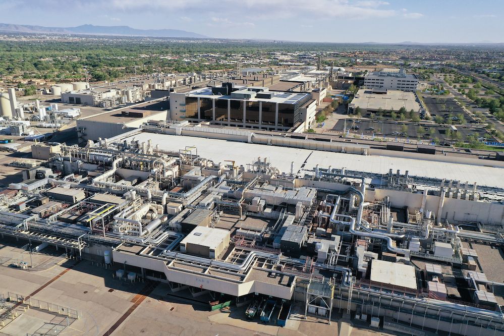
 An aerial view shows the Intel Rio Rancho campus in New Mexico, where Intel develops and manufactures technologies that optimize semiconductor packaging, memory and connectivity. On May 3, 2021, Intel announced it will invest $3.5 billion in its New Mexico operations in support of advanced semiconductor packaging technology. (Credit: Walden Kirsch/Intel Corporation)
By Jeff Rittener, Chief Government Affairs Officer at Intel
Today, Intel announced we will build on our 41-year history of investment in New Mexico by devoting $3.5 billion to equip our operations in the state for the manufacturing of advanced semiconductor packaging technologies. This expansion will create an estimated 700 high-tech jobs and 1,000 construction jobs in Rio Rancho and support an additional 3,500 jobs in the state. When taken together, the investment and the expansion of the workforce represent a significant boost to the company’s annual economic impact on New Mexico, which has been estimated at $1.2 billion (based on 2019 data). With planning activities under way and construction scheduled to begin in late 2021, Intel expects this investment to create additional economic opportunities for New Mexico.
One of the focuses of the Rio Rancho expansion is Foveros, Intel’s breakthrough 3D packaging technology that enables vertical stacking of compute tiles within a package. Advanced packaging techniques like Foveros allow integration of diverse computing engines across multiple process technologies with performance parameters similar to a single die, but with a platform scope that far exceeds the die-size limit of single-die integration. These technologies will improve product-level performance, power and area while enabling a complete rethinking of system architecture and helping to meet increasing computing needs across a variety of industries.
In the last year, the U.S. government has prioritized the development of reliable, secure and domestic sources of state-of-the-art semiconductors, with advanced packaging playing a key role. As the leading U.S. semiconductor manufacturer, Intel has contributed to that effort, most notably with the U.S. Department of Defense State-of-the-Art Heterogeneous Integration Prototype (SHIP) program and via partnership with the U.S. Defense Advanced Research Projects Agency (DARPA) to advance Application Specific Integrated Circuit (ASIC) platforms. Both of these projects take advantage of Intel’s industry-leading packaging capabilities.
Advanced packaging technology is an important part of the end-to-end semiconductor manufacturing that industry and government alike want to grow domestically. The U.S. share of global semiconductor manufacturing was 37% in 1990, but it’s just 12% today with only 9% owned by U.S. companies. The U.S. share of advanced packaging is significantly less, a paltry 2%. Strong bipartisan congressional support of the CHIPS for America Act, and President Biden’s proposal in the American Jobs Plan to fund the CHIPS Act with $50 billion, demonstrate that U.S. policymakers are committed to increasing domestic semiconductor capabilities and maintaining American technology leadership. We urge Congress to follow through on these promising beginnings by promptly and fully funding the CHIPS Act to incentivize the U.S. semiconductor industry and grow the nation’s economic and national security.
Intel is proud to be doing its part. The investment in New Mexico follows Intel’s recent announcement of a $20 billion investment two new fabs in Arizona and the unveiling of Intel’s plan to become a major provider of U.S. and Europe-based foundry capacity through our new Intel Foundry Services. Today, the Rio Rancho facilities develop and manufacture Intel® Optane™ technology, Embedded Multi-die Interconnect Bridge, and Intel® Silicon Photonics Technology, which optimize semiconductor packaging, memory, and connectivity. Adding Foveros 3D packaging technology will make our Rio Rancho site an even more important part of the restoration of U.S. semiconductor manufacturing leadership. The CHIPS Act will help increase and accelerate these types of critical domestic investments.
You must be a registered user to add a comment. If you've already registered, sign in. Otherwise, register and sign in.