- Mark as New
- Bookmark
- Subscribe
- Mute
- Subscribe to RSS Feed
- Permalink
- Report Inappropriate Content
Hi,
I'm using F-Tile Serial-Lite IV, so I need to instantiate a System PLL Clocks IP for FGT.
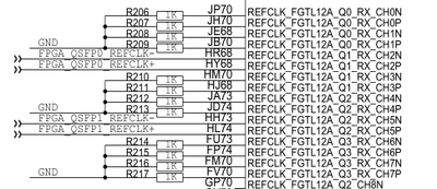
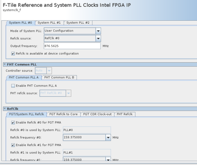
1. When select the refclk source for System PLL IP, can I choose any one of refclk source in the F-tile Reference and System PLL Clocks IP, and then enable it for FGT PMA? Since this selection is logical, and I just need to assign the input clk of PLL to physical pin in qsf? (Dont care about CDR feature.) For example, hardware design connect REFCLK_FGT_CH3 in schematic, while I can select like refclk source #0 for System PLL IP. And I then need to assign the PLL input port to the physical pin in qsf?
2. REFCLK_FGT_CH3 in schematic is differential clock input, how can I connect this differential clock to System PLL IP, since this IP has a single-ended clock input?
Link Copied
- Mark as New
- Bookmark
- Subscribe
- Mute
- Subscribe to RSS Feed
- Permalink
- Report Inappropriate Content
Hi,
There are some rules when implementing the F-Tile Reference and System PLL Clocks IP . When you enable the FGT CDR Output (RX recovered clock output), you must physically map the corresponding FGT PMA to FGT Quad 2 or 3, and you must physically map the FGT CDR Output (RX recovered clock output) to the FGT reference clock location 8 or 9 (configured as output).
For further information, you may refer to link below, Section 4.4. Guidelines for F-Tile Reference and System PLL Clocks Intel FPGA IP Usage, https://www.intel.com/content/www/us/en/docs/programmable/683872/24-1-4-8-0/guidelines-for-usage.html
Best regards,
zying
- Mark as New
- Bookmark
- Subscribe
- Mute
- Subscribe to RSS Feed
- Permalink
- Report Inappropriate Content
Hi Ziying,
thx for your reply. I'm afraid that I didnt make my question clear. I dont mean to or intended to use CDR feature. Just the PLL refclk select issue. And I've read the ug that you provided.
1. My hardware design use REFCLK_FGTL12A_Q1_RX_CH2N/P for serdes#0 and REFCLK_FGTL12A_Q1_RX_CH5N/P for serdes#1 for external clock input @156.25MHz.
1.1 When I config System PLL IP, should I instaniate one system pll IP and enable system pll#0 and #1?
1.2 When select refclk source, can i select refclk #0 and refclk #1 seperately, then enable these two refclk for FGT PMA? or I have to select refclk #2 and #5?
1.3 What are the frequency of system pll ip output signal out_refclk_fgt_x and out_systempll_clk_x? And what's the meaning of _synthlock_x signal, indicating what clock is locked?
2. How can I connect the differential clock input to the single-ended clock input port of system pll ip?
- Mark as New
- Bookmark
- Subscribe
- Mute
- Subscribe to RSS Feed
- Permalink
- Report Inappropriate Content
Hi,
1.1. When I config System PLL IP, should I instaniate one system pll IP and enable system pll#0 and #1?
>> Given that you have two different reference clock inputs for serdes#0 and serdes#1, it's advisable to instantiate one System PLL IP block and enable both System PLL#0 and System PLL#1 within that block. This configuration allows you to generate separate clock outputs for each serdes while utilizing the same System PLL IP.
1.2. When select refclk source, can i select refclk #0 and refclk #1 seperately, then enable these two refclk for FGT PMA? or I have to select refclk #2 and #5?
>> You should select refclk #2 for serdes#0 and refclk #5 for serdes#1. Each serdes requires its own dedicated reference clock to ensure proper operation and synchronization.
1.3. What are the frequency of system pll ip output signal out_refclk_fgt_x and out_systempll_clk_x? And what's the meaning of _synthlock_x signal, indicating what clock is locked?
>>The frequency of the output signals from the System PLL IP, namely out_refclk_fgt_x and out_systempll_clk_x, would depend on the specific configuration settings you choose for the PLL. Typically, you would configure the PLL to generate output frequencies that meet the requirements of your design, such as the data rate of your serial links. The _synthlock_x signal indicates whether the PLL has locked to the input reference clock signal. When _synthlock_x is asserted, it means that the PLL has achieved phase lock with the input reference clock, ensuring stable and synchronized operation.
2. How can I connect the differential clock input to the single-ended clock input port of system pll ip?
>>You may use a Differential-to-Single-Ended Converter. You can use a dedicated IC or circuitry designed to convert a differential clock signal to a single-ended clock signal.
Best regards,
zying
- Mark as New
- Bookmark
- Subscribe
- Mute
- Subscribe to RSS Feed
- Permalink
- Report Inappropriate Content
Hi,
I now transition this thread to community support. If you have a new question, feel free to open a new thread to get the support from Intel experts. Otherwise, the community users will continue to help you on this thread.
Best regards,
zying
- Subscribe to RSS Feed
- Mark Topic as New
- Mark Topic as Read
- Float this Topic for Current User
- Bookmark
- Subscribe
- Printer Friendly Page

