- Mark as New
- Bookmark
- Subscribe
- Mute
- Subscribe to RSS Feed
- Permalink
- Report Inappropriate Content
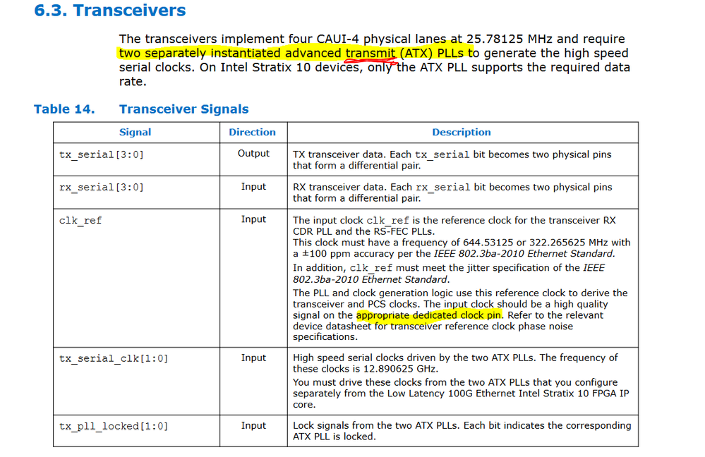
The Low Latency 100G Ethernet Intel®Stratix® 10 FPGA IP Core user guide suggest that the input reference clock pin to the ATX PLL must be a dedicated reference clock pin (2.4.2. Adding the Transceiver PLLs).
https://www.intel.com/content/dam/www/programmable/us/en/pdfs/literature/ug/ug_s10_ll_100gbe.pdf
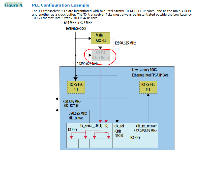
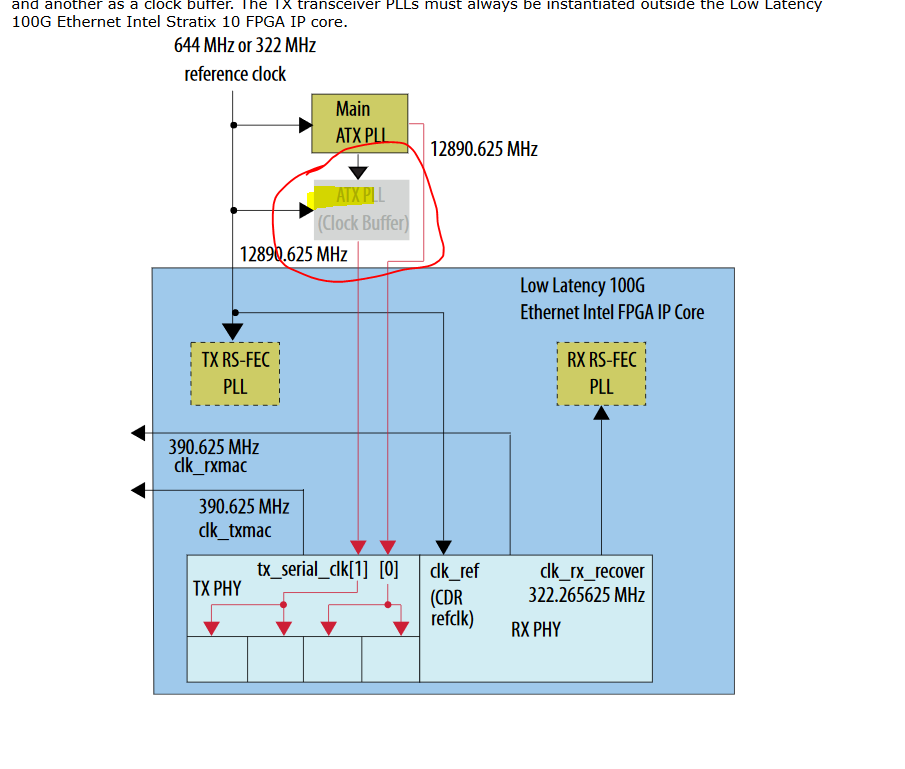
My question is: Is it okay if only one ATX PLL gets the input reference clock from the dedicated reference clock pin while the second ATX PLL merely acts as a clock buffer as shows in Figure 4.PLL Configuration Example? Also, should the pll reference clock input of the ATX PLL be tied to 0?
Link Copied
- Mark as New
- Bookmark
- Subscribe
- Mute
- Subscribe to RSS Feed
- Permalink
- Report Inappropriate Content
Hi ,
As mentioned in the user guide , in the Low Latency 100G Ethernet , have to use two ATX PLL.
- Mark as New
- Bookmark
- Subscribe
- Mute
- Subscribe to RSS Feed
- Permalink
- Report Inappropriate Content
Hi RSree,
Thanks for the reply. It would need two ATX PLLs for sure. But can one of them act as a transmit PLL to clock two GXT channels while other is being used as a clock buffer to clock the other two channels? This is shown in Figure 4.PLL Configuration Example where one of the ATX PLL is shown as a buffer.
The clock network which I am referring to is also shown in Figure 141.Main and Adjacent ATX PLL IP Instances to Drive 6 GXT Channels of
Thanks
- Mark as New
- Bookmark
- Subscribe
- Mute
- Subscribe to RSS Feed
- Permalink
- Report Inappropriate Content
- Mark as New
- Bookmark
- Subscribe
- Mute
- Subscribe to RSS Feed
- Permalink
- Report Inappropriate Content
Hi ,
I am expertise in PLL , let me check the expert in Ethernet / Transceiver and will get back to you.
- Mark as New
- Bookmark
- Subscribe
- Mute
- Subscribe to RSS Feed
- Permalink
- Report Inappropriate Content
- Mark as New
- Bookmark
- Subscribe
- Mute
- Subscribe to RSS Feed
- Permalink
- Report Inappropriate Content
Hi,
I can see that you have asked similar enquiry on another forum case
- Does an ATX PLL configured as a Clock Buffer need a reference clock of it's own or can the pll_refclk0 port be tied to ground?
and I have explained the ATX PLL clock buffer refclk connection guideline to you
Does it help or you are still confused ?
Thanks.
Regards,
dlim
- Mark as New
- Bookmark
- Subscribe
- Mute
- Subscribe to RSS Feed
- Permalink
- Report Inappropriate Content
Hi @DeshiL_Intel ,
My concern in this post is that I am using the 100G Low Latency Ethernet IP and in it's userguide, except for this diagram shown in the above figure (Figure 4), is it mentioned everywhere throughout the userguide that the input reference clock should come in through a DEDICATED REF CLOCK pin. For jitter purposes, I want to know whether the input reference clock should come in though a dedicated reference clock for both the instantiated ATX PLLs or can one these be used as a buffer as in Figure 4 shown. If we are able to use just one Reference clock input, it might save us some board routing while I want to make sure whether it is recommended or not for 100G Low Latency Ethernet IP for Stratix 10.
Pointing you to the userguide where it mentions that two "Transmit" ATX PLL should be used with reference clock input through a dedicated reference clock pin with +-100ppm accuracy:
Please note that I have underlined "transmit". I hope this is an understandable concern.
- Mark as New
- Bookmark
- Subscribe
- Mute
- Subscribe to RSS Feed
- Permalink
- Report Inappropriate Content
Actually now that I see this, the documentation just meant to use the full form of the acronym ATX where I have underlined it. Nonetheless, I still wanted to make sure whether it can be used as a buffer for this IP.
- Mark as New
- Bookmark
- Subscribe
- Mute
- Subscribe to RSS Feed
- Permalink
- Report Inappropriate Content
HI,
Yes, it can be used as clock buffer.
For reference, you can always generate the 100G example design directly from the IP core to review the design connection.
This is a better way to clarify issue rather than read through the doc.
Thanks.
Regards,
dlim
- Mark as New
- Bookmark
- Subscribe
- Mute
- Subscribe to RSS Feed
- Permalink
- Report Inappropriate Content
Hi dlim,
Thanks for checking. It was not used as a buffer in the example design. Hence I wanted to confirm.
Thanks,
Naved
- Mark as New
- Bookmark
- Subscribe
- Mute
- Subscribe to RSS Feed
- Permalink
- Report Inappropriate Content
Hi Naved,
I look deeper into the example design.
Now I understand your concern and also see where is the problem.
Basically Intel FPGA offer both soft and hard Ethernet 100G IP and so happen their example design implementation is difference
For H-tile Hard IP for Ethernet :
- The example design used 2 ATX PLL in cascading mode (as clk buffer)
For low latency 100G soft Ethernet IP :
- The example design used 2 ATX PLL as 2 separate PLL (NOT as clk buffer, just used as PLL)
Attached is the screenshot showing you the example design connection difference
Meaning low latency 100G soft Ethernet IP user guide doc - figure 4 diagram and explanation is wrong.
- I will take the action to feedback to our Intel doc team accordingly
FYI... Intel does has separate 100G soft Ethernet IP example design doc that you can refer to as well
- https://www.intel.com/content/dam/www/programmable/us/en/pdfs/literature/ug/ug-dex-s10-ll-100gbe.pdf
Finally back to your original concern, regardless which PLL mode is being used, example design always recommend to connect both PLL refclk pins to ONE same FPGA external refclk pin.
Thanks.
Regards,
dlim
- Mark as New
- Bookmark
- Subscribe
- Mute
- Subscribe to RSS Feed
- Permalink
- Report Inappropriate Content
- Mark as New
- Bookmark
- Subscribe
- Mute
- Subscribe to RSS Feed
- Permalink
- Report Inappropriate Content
Hi Naved,
After further consultation with internal team, actually both design connection also fine
- option 1 : use 2nd ATX PLL as PLL
- option 2 : use 2nd ATX PLL as clock buffer
It's just that the option 2 "use 2nd ATX PLL as clock buffer" seems to perform better as compared to option 1.
Therefore, Intel engineering team plans to amend existing example design to use option 2 in future Quartus release.
We won't be changing the user guide doc explanation anymore as it's a preferred recommendation.
Thanks.
Regards,
dlim
- Mark as New
- Bookmark
- Subscribe
- Mute
- Subscribe to RSS Feed
- Permalink
- Report Inappropriate Content
Hi @[DeshiL_Intel] ,
Thanks a lot for looking into this. From this discussion, I would summarize:
It is better to use one ATX PLL as a clock buffer while the other one being the main ATX PLL.
Based on our discussion in https://forums.intel.com/s/question/0D50P00004ZiXY6SAN/does-an-atx-pll-configured-as-a-clock-buffer-need-a-reference-clock-of-its-own-or-can-the-pllrefclk0-port-be-tied-to-ground, it would also be okay to tie the reference clock input of the ATX PLL being used as a clock buffer because it is merely being used as a buffer and would not require a clock unless we need to reconfigure it.
Please correct me if I am wrong.
Even though it is clearly mentioned in the H-Tile Hard IP for Ethernet User guide that one of the ATX PLLs is being used as a buffer, the 100G Low Latency User guide does not specify that it is okay to use it other than Figure 4.
Thanks,
Naved
- Mark as New
- Bookmark
- Subscribe
- Mute
- Subscribe to RSS Feed
- Permalink
- Report Inappropriate Content
HI Naved,
Your summary got it all correct.
Sometime doc can't fully explained thing clearly and there maybe changes from time to time.
That's why we have this Intel forum platform to help clarify issue with customer.
I hope I have clear your doubt now.
Have a nice day. :)
Thanks !
Regards,
dlim
- Mark as New
- Bookmark
- Subscribe
- Mute
- Subscribe to RSS Feed
- Permalink
- Report Inappropriate Content
HI Naved,
Just want to close loop with you on this issue to set this case to closure since the ATX PLL usage model has been clarified.
For now, I am setting this case to closure.
Thanks.
Regards,
dlim
- Subscribe to RSS Feed
- Mark Topic as New
- Mark Topic as Read
- Float this Topic for Current User
- Bookmark
- Subscribe
- Printer Friendly Page


