- Mark as New
- Bookmark
- Subscribe
- Mute
- Subscribe to RSS Feed
- Permalink
- Report Inappropriate Content
Hello,
In the user guide, with H-tile types - Gen3x8, application clock or coreclkout_hip frequency = 250 MHz. But I could not verify it in the TA clock report.
Instead, I could see
"dut|dut|hip|altera_pcie_s10_hip_ast_pipen1b_inst|altera_pcie_s10_hip_ast_pllnphy_inst|g_phy_g3x8.phy_g3x8|phy_g3x8|xcvr_hip_native|ch0"
and its frequency is 500 MHz.
It matches the constraints below:
set clk_source_freq "250.0 MHz"
set datarate_100m  80
...
# 500M for  aibx2 clocks if BW less or equal 64G
} elseif { [expr $datarate_100m * 8] <= 640 }  {
  dict set multiply_factor_dict aib_internal_div 2
  dict set divide_factor_dict   aib_internal_div 1
  dict set multiply_factor_dict clkout 1
  dict set divide_factor_dict   clkout 1
}
...

create_generated_clock \
              -name  $inst|xcvr_hip_native|ch${channels} \
              -source $no_inst_tx_internal_div_reg \
              -master_clock $tx_internal_div_reg_name \
              -multiply_by [dict get $multiply_factor_dict clkout] \
              -divide_by   [dict get $divide_factor_dict   clkout] \
              $no_inst_tx_clkout -add
I think this clock is transport-layer clock and it is used to derive application clock/ coreclkout_hip / pld_clk250 as in the code below
assign  coreclkout_hip = enable_512adapter_hwtcl? pld_clk250                : coreclkout_hip_wire    ;
...

altera_ep_g3x16_avst512_io_pll_s10 altera_avst512_iopll (
		.outclk_0      (pld_clk250),
		.refclk        (coreclkout_hip_wire),
		.rst           (~pin_perst),
        .locked        (iopll_locked),
        .permit_cal    (serdes_pll_locked_wire)
	);
Do I understand it correctly?
If it is correct, then, it is confusing to me. Here is what I found.
I use application clock / coreclkout_hip as the refclk of PLL to derive another clock domain (200 MHz). The setting of PLL is
- Reference clock = 250 MHz
- Output clock = 200 MHz
However, when re-check the TA clock report:
- Reference clock = 500 MHz
- Output clock = 400 MHz
what is wrong here?
My platform is Stratix 10 MX | Quartus Prime Pro ver 22.2
Thank you,
TN
- Mark as New
- Bookmark
- Subscribe
- Mute
- Subscribe to RSS Feed
- Permalink
- Report Inappropriate Content
Hi,
I think that indicates the Clock Fmax.
If you changed the optimization Mode from Balanced to Aggressive Area you can achieve the 500MHz.
The Fmax specification is based on the fast clock used for serial data.
The interface Fmax is also dependent on the parallel clock domain which is design dependent and requires timing analysis.
Hope this clarified.
Regards,
Wincent_Intel
Link Copied
- Mark as New
- Bookmark
- Subscribe
- Mute
- Subscribe to RSS Feed
- Permalink
- Report Inappropriate Content
Hi,
The frequency of coreclkout_hip is for gen3x8 is 250 MHz as per mention in the user guide.
Are you using the design example provided in Quartus ?
Can you check if you enable two clock together ?
Regards,
Wincent_Intel
- Mark as New
- Bookmark
- Subscribe
- Mute
- Subscribe to RSS Feed
- Permalink
- Report Inappropriate Content
Hi Wincent,
I used the example design provided in Quartus. Running PIO transfer, gencheck, loopback seem OK.
Then, I want to insert our accelerators to receive data from the HOST, doing computations, and send back results to the HOST.
I want to run these accelerators at a lower frequency (200MHz), so I pulled PLL core which uses coreclkout_hip as the reference clock.
But when re-checking TA clock report, it showed the output clock freq = 400 MHz and refclk = 500 MHz
@Wincent_Altera wrote:Can you check if you enable two clock together ?
Could you clarify this? I could not see where to enable two clocks when pulling the MCDMA IP Core.
There is only 1 selection regarding frequency: "PCIe gen3 x8 - 250 MHz"
Thanks,
TN
- Mark as New
- Bookmark
- Subscribe
- Mute
- Subscribe to RSS Feed
- Permalink
- Report Inappropriate Content
Hi,
Can you please provide me the printscreen of the TA report that mentioning 500 MHz ?
Regards,
Wincent_Intel
- Mark as New
- Bookmark
- Subscribe
- Mute
- Subscribe to RSS Feed
- Permalink
- Report Inappropriate Content
Hi,
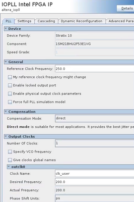
Sure! This is the PLL configuration
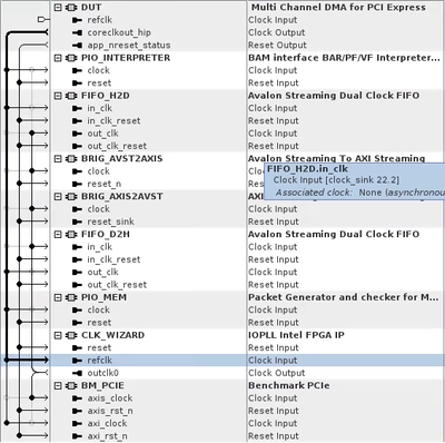
And the system view with clock interfaces
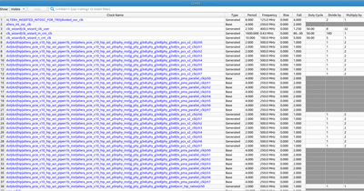
And this is what clock report with the final snapshot
- clkout of the IOPLL
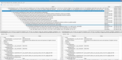
- And clock network report
Regards,
TN
- Mark as New
- Bookmark
- Subscribe
- Mute
- Subscribe to RSS Feed
- Permalink
- Report Inappropriate Content
Hi,
I think that indicates the Clock Fmax.
If you changed the optimization Mode from Balanced to Aggressive Area you can achieve the 500MHz.
The Fmax specification is based on the fast clock used for serial data.
The interface Fmax is also dependent on the parallel clock domain which is design dependent and requires timing analysis.
Hope this clarified.
Regards,
Wincent_Intel
- Mark as New
- Bookmark
- Subscribe
- Mute
- Subscribe to RSS Feed
- Permalink
- Report Inappropriate Content
Hi,
Thanks for your clarification.
So, how could I review the actual clock frequency?
Regards,
TN
- Mark as New
- Bookmark
- Subscribe
- Mute
- Subscribe to RSS Feed
- Permalink
- Report Inappropriate Content
Hi,
The way you review the clock frequency at the first post shall be correct as per mention in the user guide.
Regards,
Wincent_Intel
- Mark as New
- Bookmark
- Subscribe
- Mute
- Subscribe to RSS Feed
- Permalink
- Report Inappropriate Content
Hi,
Thanks for your help.
That means:
In this case, we could not see the actual clock frequency in the Timing Analysis report, and the only way to know the exact number is by reviewing the code.
Is that correct?
Thanks and Regards,
TN
- Mark as New
- Bookmark
- Subscribe
- Mute
- Subscribe to RSS Feed
- Permalink
- Report Inappropriate Content
Would expect to see actual PLL frequencies in timing analysis report under "clocks" and also in synthesis report under Resources/PLLs.
- Mark as New
- Bookmark
- Subscribe
- Mute
- Subscribe to RSS Feed
- Permalink
- Report Inappropriate Content
Hi,
Thanks for your reply!
That is why I was confused.
Under "Clock" report in Timing Analysis, it showed 'output_clk" of PLL is 400 MHz.
Meanwhile, my setting ratio of PLL is 'refclk/output_clk' = 250MHz/ 200MHz
That's why I thought refclk frequency should be: 500 MHz, and it violates the user guide where the frequency should be 250 MHz.
Thanks and Regards,
TN
- Mark as New
- Bookmark
- Subscribe
- Mute
- Subscribe to RSS Feed
- Permalink
- Report Inappropriate Content
Hi,
Glad that you get your answer.
So do you still have any further questions on this forum case ? Or everything is nice ?
if yes, I shall close this case from my place and leave this thread to the public community.
Regards,
Wincent_Intel
- Mark as New
- Bookmark
- Subscribe
- Mute
- Subscribe to RSS Feed
- Permalink
- Report Inappropriate Content
Hi,
Thanks for your reply. Could you please make this case open?
After @FvM reply, I have checked the actual frequency of PLL output_clk = 400 MHz.
With the setup ratio 250MHz/200MHz, it expects "coreclkout_hip" should be 500 MHz instead of 250 MHz.
Therefore, I still need to discuss more to know what I was wrong.
Thanks and Regards,
TN
- Mark as New
- Bookmark
- Subscribe
- Mute
- Subscribe to RSS Feed
- Permalink
- Report Inappropriate Content
Hi,
the printscreen is not clear, could you please provide again ?
so that I can confirm the issue ?
Regards,
Wincent_Intel
- Mark as New
- Bookmark
- Subscribe
- Mute
- Subscribe to RSS Feed
- Permalink
- Report Inappropriate Content
Hi,
Here is the screenshot of clock report
The clk_wizard_clk_user is output_clk of PLL.
And, this is my PLL setting
Thanks and Regards,
TN
- Mark as New
- Bookmark
- Subscribe
- Mute
- Subscribe to RSS Feed
- Permalink
- Report Inappropriate Content
Hi,
Apologize for late reply due to holiday.
Based on the user guide, the maximum H-tile types - Gen3x8, application clock is 250 MHz.
I dont understand your statement as "With the setup ratio 250MHz/200MHz, it expects "coreclkout_hip" should be 500 MHz instead of 250 MHz."
Can you please clarified more on this ?
by logic when you set it as 250 why it shall get 500 MHz instead of 250Mhz ?
Regards,
Wincent_Intel
- Mark as New
- Bookmark
- Subscribe
- Mute
- Subscribe to RSS Feed
- Permalink
- Report Inappropriate Content
Hi,
There is some reason the frequency is double.
I suggest you to check the RTL design and see what is connected to the output.
I am not an expert in timing issues, As I am supporting PCIe design in most of the time.
Another suggestion to get better support is open a new case with title and category related to timing.
So that the correct expert will be assigned to help you.
Do attach the .qar and timing report for that.
Regards,
Wincent_Intel
- Mark as New
- Bookmark
- Subscribe
- Mute
- Subscribe to RSS Feed
- Permalink
- Report Inappropriate Content
Hi,
There are no timing issues (setup or hold time violation yet)
I made a simple system that is
MCDMA => DC-FIFO => DC-FIFO => MCDMA
I observed the same behavior @output clock of PLL. That means "coreclkout_hip" frequency should be 500 MHz.
Could you please suggest which sub-forum should I post the question regarding this?
Regards,
TN
- Mark as New
- Bookmark
- Subscribe
- Mute
- Subscribe to RSS Feed
- Permalink
- Report Inappropriate Content
Hi,
Can you share the .qar file with me ?
So that I can help to look at ur design.
Regards,
Wincent_Intel
- Mark as New
- Bookmark
- Subscribe
- Mute
- Subscribe to RSS Feed
- Permalink
- Report Inappropriate Content
Hi,
Sure, this is the design I mentioned.
My Quartus version is 22.2
Regards,
TN
- Mark as New
- Bookmark
- Subscribe
- Mute
- Subscribe to RSS Feed
- Permalink
- Report Inappropriate Content
Hi Wincent,
No problem.
My mistake ... the statement might not be clear. Here is the scenario:
- The ratio of PLL 250MHz/200MHz" - I expected input clk = 250 MHz and output clock = 200 MHz
- However, I observed the actual frequency of PLL output clk is 400 MHz
=> Hence, my implication is the input frequency is 500 MHz which means coreclkout_hip = 500 MHz instead of 250MHz as stated in the user guide.
---
The output clock which is fed to a DC-FIFO also results the same frequency.
Regards,
TN
- Subscribe to RSS Feed
- Mark Topic as New
- Mark Topic as Read
- Float this Topic for Current User
- Bookmark
- Subscribe
- Printer Friendly Page


