- Mark as New
- Bookmark
- Subscribe
- Mute
- Subscribe to RSS Feed
- Permalink
- Report Inappropriate Content
Hi,
We are using Quartus 24.1 to compile the type 3 ddr memory design example for the board and program the FPGA using the following guide:
Agilex™ 7 R-Tile Compute Express Link* (CXL*) FPGA IP Design Example User Guide version 1.12 for quartus 24.1.
If we program it with the recommended SW4 switch setting (4.1 ON), it does not work and we loose access to the FPGA with a JTAG chain broken error (same as this https://community.intel.com/t5/Programmable-Devices/JTAG-error-after-programming-device/td-p/1594877)
The same happens if we leave SW4 to the preset configuration (4.3 ON).
If we program the device with all SW4 pins to OFF (as it was for the R1BES version of the board) we can still detect the FPGA but programming fails with the attached configuration errors. The description states: "External hardware access error. The first i2c command has failed, no response from voltage regulator".
Could you please let me know what is the correct SW4 setting and how we should proceed?
Best Regards,
Alverti Chloe
Best Regards,
Chloe
- Mark as New
- Bookmark
- Subscribe
- Mute
- Subscribe to RSS Feed
- Permalink
- Report Inappropriate Content
Hi again,
The problem was on the PCIe slot on the server side.
We replaced our card and the problem was fixed.
For anyone facing the same problems, we had to check the x16 slot with other devices to identify the lane drop issue in BIOS.
CXL IP designs apparently are note recognized in BIOS as PCIe devices even when the design is working -- the corresponding PCIe slot always shows the message "Link did not train" -- as if nothing is attached on the slot.
Thank you for your help,
Chloe
Link Copied
- Mark as New
- Bookmark
- Subscribe
- Mute
- Subscribe to RSS Feed
- Permalink
- Report Inappropriate Content
Hi Chloe,
I see. The sw4 should be all off. The error u see about I2C is caused the wrong setting in PMBUS. U can check it in Quartus->Assignment->Device->Device and Pin option, the setting of SCL and SDA in Configuration->Configuration pin option; the setting of VR in Power Management.
The right setting can refer from the setting in example design. Or give me u specific opn of your board, let me check it.
Best regards,
WZ
- Mark as New
- Bookmark
- Subscribe
- Mute
- Subscribe to RSS Feed
- Permalink
- Report Inappropriate Content
Hi,
Thank you very much for your reply!
So this means that the Table 32 in the document is incorrect?
If so could you please then let me know what SW3 should be set to?
Setting SW4 to all off did not make the problem go away.
With respect to the other settings, shouldn't they be already correct? I am compiling the example design for the device.
Our board opn is DK-DEV-AGI027RBES. And we are compiling the type 3 example design for this board.
Best,
Chloe
- Mark as New
- Bookmark
- Subscribe
- Mute
- Subscribe to RSS Feed
- Permalink
- Report Inappropriate Content
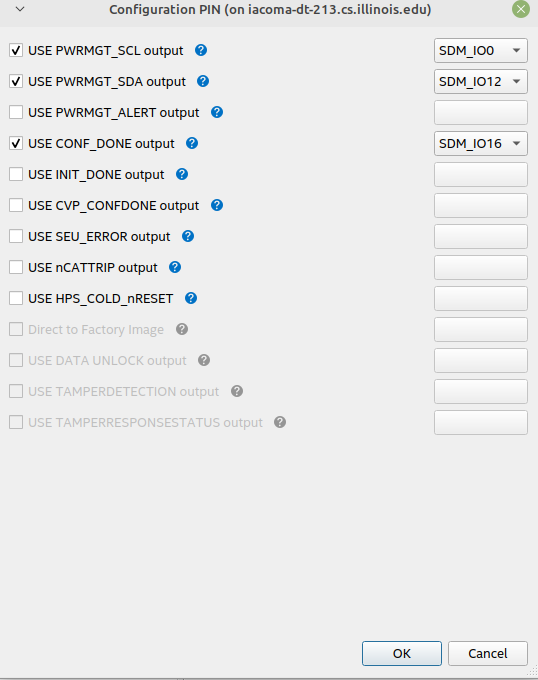
I am attaching some screenshots from our configuration in case that helps.
Thank you,
Chloe
- Mark as New
- Bookmark
- Subscribe
- Mute
- Subscribe to RSS Feed
- Permalink
- Report Inappropriate Content
Hi again,
Are there any thoughts on this? Because we are stuck and we cannot really move forward.
Thank you very much for your help!
Best Regards,
Chloe
- Mark as New
- Bookmark
- Subscribe
- Mute
- Subscribe to RSS Feed
- Permalink
- Report Inappropriate Content
Hi there,
I check the setting in quartus is no error, please set all switch to their default setting(just like User guire )
https://www.intel.com/content/www/us/en/docs/programmable/683288/current/default-settings.html
SW4 should be all off, it can enable sdm_pmbus signal and communicate with Voltage regulator.

Best regards,
WZ
- Mark as New
- Bookmark
- Subscribe
- Mute
- Subscribe to RSS Feed
- Permalink
- Report Inappropriate Content
Sorry for the miss, for RBES, sw4 should be off off on off


- Mark as New
- Bookmark
- Subscribe
- Mute
- Subscribe to RSS Feed
- Permalink
- Report Inappropriate Content
If you see our first post you will read that we have tried this already.
If we go with off/off/on/off we get a jtag chain error. If we go fro off/off/off/off we have the errors you see above.
Also please keep in mind that it seems that for CXL IP designs the switches are not the same as the user guide.
We are following this guide --> Agilex™ 7 R-Tile Compute Express Link* (CXL*) FPGA IP Design Example User Guide version 1.12 for quartus 24.1.
Please give us some advice how to solve this.
Chloe
- Mark as New
- Bookmark
- Subscribe
- Mute
- Subscribe to RSS Feed
- Permalink
- Report Inappropriate Content
Hi,
I have managed to solve the issue of voltage regulator error and the device is in USER MODE after programming.
However, still I cannot detect 0ddb with lspci and the design is not working.
What should I do?
Thank you,
Chloe
- Mark as New
- Bookmark
- Subscribe
- Mute
- Subscribe to RSS Feed
- Permalink
- Report Inappropriate Content
- Mark as New
- Bookmark
- Subscribe
- Mute
- Subscribe to RSS Feed
- Permalink
- Report Inappropriate Content
Hi there,
I need to confirm a few pieces of information with you:
- What was the cause of the previous issue with the PMBUS on the board?
- Have you tried the PCIe Gen5 example design and did it train successfully (because PCIe is more general)?
Best regards,
WZ
- Mark as New
- Bookmark
- Subscribe
- Mute
- Subscribe to RSS Feed
- Permalink
- Report Inappropriate Content
Hi,
- I set all switches to the values you state above that however do not match the "(CXL*) FPGA IP Design Example User Guide", and I set all device configuration values of the cxl design to the ones found in the devkit examples.
- Yes I have compiled and run the PCIe Gen5 example design and it trains successfully and the card is found via "lspci".
Best,
Chloe
- Mark as New
- Bookmark
- Subscribe
- Mute
- Subscribe to RSS Feed
- Permalink
- Report Inappropriate Content
One difference for the example the PCie link width is x8 while for the CXL IP it is x16.
Please tell me how I should move forward.
Best Regards,
Chloe
- Mark as New
- Bookmark
- Subscribe
- Mute
- Subscribe to RSS Feed
- Permalink
- Report Inappropriate Content
Hi there,
Here are some suggestions:
- Please confirm that your CPU and PCIe slots support CXL.
- For BIOS settings, you can refer to section 6.2 in the Agilex™ 7 R-Tile Compute Express Link* (CXL*) FPGA IP Design Example User Guide.
- If the above settings are all correct, I recommend using the debug tool kit. It can help you observe where your training is getting stuck. For using the debug tool kit, you can refer to section 5.1 in the Agilex™ 7 R-Tile Compute Express Link* (CXL*) 1.1/2.0 FPGA IP User Guide.
Best regards,
WZ
- Mark as New
- Bookmark
- Subscribe
- Mute
- Subscribe to RSS Feed
- Permalink
- Report Inappropriate Content
Hi there,
Do we have some progress on this issue?
Best regards,
WZ
- Mark as New
- Bookmark
- Subscribe
- Mute
- Subscribe to RSS Feed
- Permalink
- Report Inappropriate Content
Hi,
Thank you for your reply -- We are trying to figure out if it is a server problem as you pointed out.
Our server is CXL compatible but we may face a PCIe drop lane issue.
As a clarification the CXL IP cannot tolerate 8 lanes on the PCIe slot, right?
I will keep you posted once we have figured out.
Best,
Chloe
- Mark as New
- Bookmark
- Subscribe
- Mute
- Subscribe to RSS Feed
- Permalink
- Report Inappropriate Content
Hi again,
The problem was on the PCIe slot on the server side.
We replaced our card and the problem was fixed.
For anyone facing the same problems, we had to check the x16 slot with other devices to identify the lane drop issue in BIOS.
CXL IP designs apparently are note recognized in BIOS as PCIe devices even when the design is working -- the corresponding PCIe slot always shows the message "Link did not train" -- as if nothing is attached on the slot.
Thank you for your help,
Chloe
- Subscribe to RSS Feed
- Mark Topic as New
- Mark Topic as Read
- Float this Topic for Current User
- Bookmark
- Subscribe
- Printer Friendly Page