- Mark as New
- Bookmark
- Subscribe
- Mute
- Subscribe to RSS Feed
- Permalink
- Report Inappropriate Content
[EDIT] SOLVED
Hello, I'm trying to develop an accelerator for a computer vision algorithm. The host program is running on the Intel Atom on the DE2i-150 board, and is sending images to the FPGA for processing. The problem is that I can't get more than 3 to 10MB/s throughput, which is quite small since the PCI-Express should be able to deliver something about 250MB/s, and the SDRAM should be even faster. My QSYS is pretty simple, you could see it on the attachment. I would appreciate if someone could help me with this. Is that a common issue? Can I be able to get more speed, something like 90MB/s or so? If so, how could I accomplish that? Many thanks.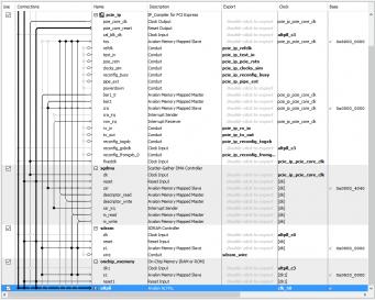
Link Copied
- « Previous
-
- 1
- 2
- Next »
- Mark as New
- Bookmark
- Subscribe
- Mute
- Subscribe to RSS Feed
- Permalink
- Report Inappropriate Content
It's a DE2i-150, which holds a EP4CGX150DF31C7 fpga.
I've tried putting together what you have said, but the same problem happened on the board. Except that this time, the BIOS does not seem to be loading anymore, since the self test is not running anymore (or at least, the buzzer is not buzzing). And I don't know how to fix it. Ive already tried removing the BIOS battery, which worked last time. The FPGA is still working (I can upload other designs into it), which makes me think that it was not a pinning problem or anything like that. I have no idea what may have caused it. Just the fact that I've splitted the SGDMA into a mSDGMA caused that. Funny thing is that the last design that you have sent is supposed to run on this exact same board. But I've noticed one slight detail on the pin planner. On this design, they use the HSMC reserved clock as an 125MHz clock. I think that's not allowed, as I've looked into the board system manual and it says there that it's a "Dedicated clock input" for the HSMC. This incompatibility does not make sense for me. I'm not sure how to proceed now. I've already contacted the TERASIC support.- Mark as New
- Bookmark
- Subscribe
- Mute
- Subscribe to RSS Feed
- Permalink
- Report Inappropriate Content
OK even though the board is different the Cyclone IV GX example should still work. One thing I noticed is that you are using the SDRAM controller IP for your memory, but this board has DDR3. So you need to be using the altmemphy IP for DDR3 (https://www.altera.com/ja_jp/pdfs/literature/hb/external-memory/emi_ddr3_ug.pdf)
That is also contributing to the slow throughput.- Mark as New
- Bookmark
- Subscribe
- Mute
- Subscribe to RSS Feed
- Permalink
- Report Inappropriate Content
Hmm, I will check this out too.
I'm still stuck with the problem, starting to think that the Atom bricked somehow.- Mark as New
- Bookmark
- Subscribe
- Mute
- Subscribe to RSS Feed
- Permalink
- Report Inappropriate Content
(sorry for the double post)
- Mark as New
- Bookmark
- Subscribe
- Mute
- Subscribe to RSS Feed
- Permalink
- Report Inappropriate Content
Sorry to hear about your BIOS. From what I've read online, people usually take out the battery for 5 - 10 minutes and then after putting it back in, the BIOS should work again.
- Mark as New
- Bookmark
- Subscribe
- Mute
- Subscribe to RSS Feed
- Permalink
- Report Inappropriate Content
Yes, that's what I've done before. Now it's not working. I think it's a huge flaw that this board does not have any built in bios flash mechanism or something like that.
The problem is very similar to this one: http://www.alteraforum.com/forum/showthread.php?t=42694&highlight=de2i-150+bios- Mark as New
- Bookmark
- Subscribe
- Mute
- Subscribe to RSS Feed
- Permalink
- Report Inappropriate Content
Also, after some research I've found this framework, which seems to be pretty good: http://riffa.ucsd.edu/
Have someone else tried it? I believe it should work on the DE2i- Mark as New
- Bookmark
- Subscribe
- Mute
- Subscribe to RSS Feed
- Permalink
- Report Inappropriate Content
krasner and dsl,
Thank you very much for your help. I have figured it out how to fix the board. Just left it resting without the battery for the weekend and on the morning it simply worked. That being said, the RIFFA solution worked very very well: https://www.alteraforum.com/forum/attachment.php?attachmentid=10992 So if there's someone who has a board that can use this framework, go for it! Works like a charm, and it abstracts the PCIe from your verilog code too: --- Quote Start --- On the hardware side, users access an interface with independent transmit and receive signals. The signals provide transaction handshaking and a first word fall through FIFO interface for reading/writing data. No knowledge of bus addresses, buffer sizes, or PCIe packet formats is required. Simply send data on a FIFO interface and receive data on a FIFO interface. RIFFA does not rely on a PCIe Bridge and therefore is not subject to the limitations of a bridge implementation. Instead, RIFFA works directly with the PCIe Endpoint and can run fast enough to saturate the PCIe link. Both the software and hardware interfaces have been greatly simplified. --- Quote End --- :) :) :)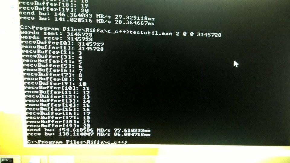
- Mark as New
- Bookmark
- Subscribe
- Mute
- Subscribe to RSS Feed
- Permalink
- Report Inappropriate Content
Great to hear that!!! Can you post your project, if you're ok with it?
- Mark as New
- Bookmark
- Subscribe
- Mute
- Subscribe to RSS Feed
- Permalink
- Report Inappropriate Content
If you mean to post the quartus project, I didn't make anything yet. I was trying to figure out this PCIe problem first.
The riffa works pretty well out of the box. You just have to follow the tutorial to create some cores that don't come with the package. Pretty straightforward. If you mean what my project is about, it is basically an interactive Datashow projector using computer vision.- Mark as New
- Bookmark
- Subscribe
- Mute
- Subscribe to RSS Feed
- Permalink
- Report Inappropriate Content
Kinda late to this thread (Apologies).
RIFFA should work for any of the Altera PCIe development boards -- If it's not included in the RIFFA distribution, it's just because we haven't tested it -- ping me and I'll help you out. riffa.ucsd.edu and https://github.com/drichmond/riffa- Subscribe to RSS Feed
- Mark Topic as New
- Mark Topic as Read
- Float this Topic for Current User
- Bookmark
- Subscribe
- Printer Friendly Page
- « Previous
-
- 1
- 2
- Next »