- Mark as New
- Bookmark
- Subscribe
- Mute
- Subscribe to RSS Feed
- Permalink
- Report Inappropriate Content
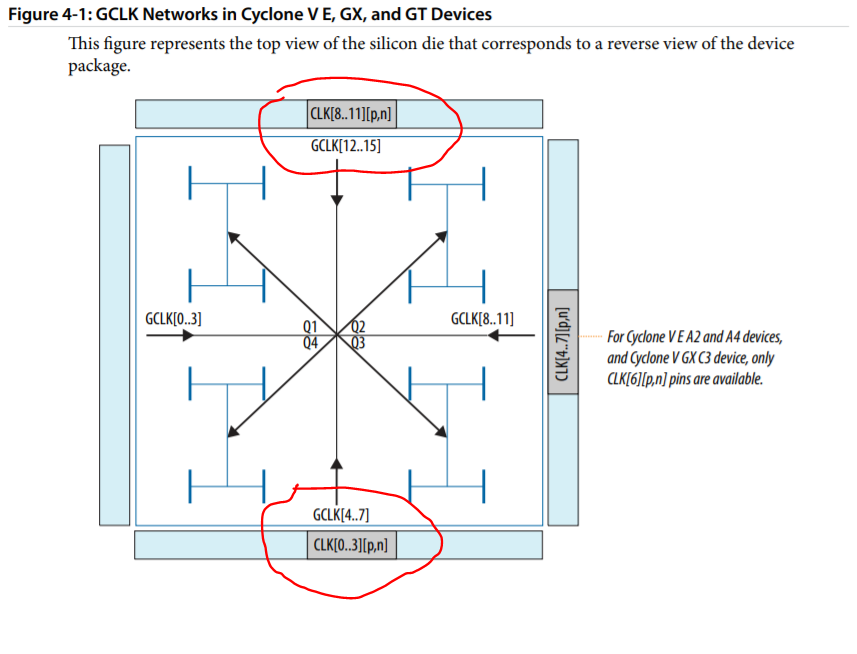
From reading various documents and the position of the 8 PLLs in the 5CEFA9F31C7 device I am using and their connection to physical clock pins there is no way to provide the reference clock input to both the top and bottom hard memory controllers from a single clock pin. Is this correct, or am I missing something?
- Tags:
- Cyclone® V FPGAs
Link Copied
- Mark as New
- Bookmark
- Subscribe
- Mute
- Subscribe to RSS Feed
- Permalink
- Report Inappropriate Content
Hi Sir,
Yes, you are right. There is a dedicated clock input pin to the GCLK network as shown below. For the clock input pin connection to GCLK, you may refer to Table 4-2 under "Chapter 4 Clock Networks and PLLs in Cyclone V Devices" --> https://www.intel.com/content/dam/www/programmable/us/en/pdfs/literature/hb/cyclone-v/cv_5v2.pdf
In the handbook also mentioned that driving a PLL over a global or regional clock can lead to higher jitter at the PLL input, and the PLL will not be able to fully compensate for the global or regional clock. Intel recommends using the CLK<#>p pins for optimal performance when you use single-ended clock inputs to drive the PLLs.
Hope this helps.
Thanks
Regards,
Aida
- Subscribe to RSS Feed
- Mark Topic as New
- Mark Topic as Read
- Float this Topic for Current User
- Bookmark
- Subscribe
- Printer Friendly Page
