Design Example: Achieving Timing Closure When Using Top I/O Sub Bank in Intel Agilex® devices
Success! Subscription added.
Success! Subscription removed.
Sorry, you must verify to complete this action. Please click the verification link in your email. You may re-send via your profile.
- Intel Community
- Intel Community Knowledge Base
- Product Support Forums Knowledge Base
- FPGA Knowledge Base
- FPGA Wiki
- Design Example: Achieving Timing Closure When Using Top I/O Sub Bank in Intel Agilex® devices
Design Example: Achieving Timing Closure When Using Top I/O Sub Bank in Intel Agilex® devices
- Subscribe to RSS Feed
- Mark as New
- Mark as Read
- Bookmark
- Subscribe
- Printer Friendly Page
- Report Inappropriate Content
1. Introduction/Overview
Intel Agilex® devices have general-purpose I/O banks located at the top and bottom of the device. Each I/O bank has two sub-banks. The top I/O sub-bank is located near to the edge of the die, while the bottom sub-bank is located near the FPGA core. Each sub-bank has a dedicated I/O PLL and four I/O lanes with 12 I/O pins in each lane for you to design your general-purpose I/O (GPIO) applications.
When using the top I/O sub-bank for GPIO applications, you may see timing violations on the half-cycle transfer from the input data pins to the FPGA core due to the long data path. The pins in the top I/O sub-banks have been identified as pin index 48 to 95 in the device pin-out files.
This design example exemplifies the setup timing violation that occurs when using the top I/O sub-bank for GPIO applications and two methods to resolve this timing violation using the GPIO Intel® FPGA IP.
2. Requirements
2.1 Hardware Requirements
There is no hardware requirement for this example design. The link to download the example design can be accessed at https://www.intel.com/content/www/us/en/design-example/714634/intel-agilex-7-fpga-an911-achieving-timing-closure-when-using-top-i-o-sub-bank.html
2.2 Software Requirements
The software tool where this example design is created and tested is Intel® Quartus® Prime Pro Edition Software version 20.3.
3 Walkthrough [For application note with reference design]
3.1 Hardware Setup
No hardware setup is required for this example design since the design is a Non-kit specific Intel Agilex® FPGA F-Series Design Example.
3.2 Software Setup
The downloaded file for this design example is an911_design_examples.par. Upon extracting the .par file, there will be three design example revisions namely
- top – original design example with setup timing violation.
- top_w1 – design example using negative edge clock latching solution.
- top_w2 – design example using half-rate transfer mode solution.
All three revisions are created using the Intel Agilex® AGFA014R24A3E3V device in Intel Quartus® Prime Pro Edition Software version 20.3. To compile the .par, follow the instruction below:
- Extract the design with these two steps:
- quartus_sh --platform_install -package an911_design_examples.par
- quartus_sh --platform -name an911_design_examples -search_path devplatforms/20.1.0/an911_design_examples
- Compile the design consecutively:
- quartus_sh –flow compile top -c top
- quartus_sh –flow compile top -c top_w1
- quartus_sh –flow compile top -c top_w2
- Compare the timing reports between these three revisions.
- top.sta.rpt
- top_w1.sta.rpt
- top_w2.sta.rpt
4. Concept
4.1 GPIO Intel® FPGA IP Architecture
The design example focuses on the input data paths from the GPIO Intel® FPGA IP to the FPGA core. The GPIO Intel FPGA IP comprises of three components:
- Double data rate input/output (DDIO) — halves or doubles the data rate of a communication channel.
- Delay chains — configure the delay chains to perform specific delays and assist in I/O timing closure.
- I/O buffers — connect the pads to the FPGA.
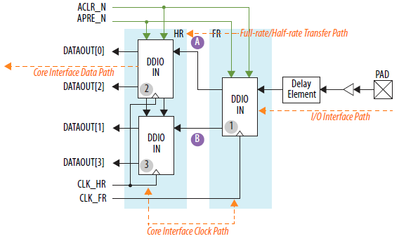
The GPIO Intel®FPGA IP has Double Data Rate I/O (DDIO) blocks in the input path (DDIO IN) and DDIO blocks in the output path (DDIO OUT). Each path consists of one full-rate DDIO block (FR DDIO IN) and two half-rate DDIO blocks (HR DDIO IN). The subsequent content in this document focuses only on the input data path of the GPIO Intel FPGA IP.
The following diagram shows the input data path of the GPIO Intel FPGA IP. The pad receives the data, and the FR DDIO IN (1) block captures data on the rising and falling edges of the ck_fr clock. The data is sent through signals (A) and (B) to HR DDIO IN blocks. HR DDIO IN (2) and HR DDIO IN (3) blocks halve the data rate and present the data through dout[3:0].
Figure 1: Timing Components of A Simplified GPIO Input Path
5. Results
5.1 Compiling the top design revision
The top.bdf design example shows the connections of the GPIO Intel FPGA IP input data pins assigned to PIN CT57 in the top I/O sub-bank. The DDIO IN pins are connected to the FPGA core registers, and the registers use a positive edge clock for data sampling. In this design example, the GPIO Intel FPGA IP is set to full-rate data transfer with a clock frequency of 250 MHz. The clock is provided by outclk0.
Figure 2: Block Diagram of Full-rate Data Transfer from DDIO IN to FPGA Core

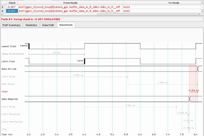
The following figure shows setup violations from the DDIO IN pins to the FPGA core registers. The latch clock occurs at half-cycle of the launch clock with only 2 ns setup requirement. However, the data arrival time is a longer time than the data required time.
Figure 3: Setup Violation Timing Waveform
To resolve this violation, you can use one of the following solutions, which are included in the design example:
- top_w1
Using a falling edge clock for data capturing in the full-rate transfer mode. This solution lets your design to operate at maximum GPIO clock frequency but requires changes to the clock in user logic.
- top_w2
Using GPIO Intel FPGA IP in half-rate transfer mode. This solution operates in a slower clock frequency without changing the user logic clock.
5.2 Compiling the top_w1 design revision
As shown in the Timing Components of A Simplified GPIO Input Path figure, the full-rate transfer mode is represented by signals A and B. In the full-rate mode interface, the two signals bypass the half-rate block. The timing violation on half-cycle transfer from the GPIO Intel FPGA IP to the FPGA core is due to a tighter setup slack. To rectify this, use a falling edge clock to capture the data because the full cycle window provides more setup slack to fulfill the timing, as shown in the top_w1 design example.
Figure 4: Block Diagram of Falling Edge Clock Core Register

The following figure shows the timing waveform of the design example using a falling edge clock. The latch clock now has a full cycle window of 4 ns to capture the input data.
Figure 5: Timing Waveform for Setup Time Using Falling Edge Clock
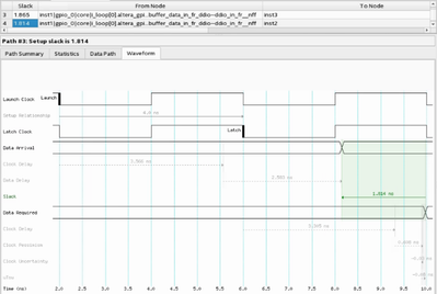
This solution provides a setup margin of 1.814 ns with no additional latency to the design.
5.3 Compiling the top_w2 design revision
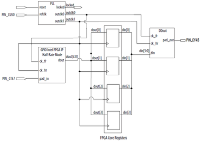
As shown in the Timing Components of A Simplified GPIO Input Path figure, in a half-rate mode interface, A and B signals go through the HR DDIO IN block and output as DATAOUT[0:3]. Transferring data in half-rate mode reduces the core frequency, thus relaxing the setup slack. However, this requires design modifications by changing the GPIO Intel FPGA IP to half-rate mode. The top_w2 design example shows the full implementation of this solution. The outclk0 provides 250 MHz as the full-rate frequency, and the outclk1 provides 125 MHz as the half-rate frequency.
Figure 6: Block Diagram of Half-rate Mode Implementation
The following figure shows the timing waveform for the FR DDIO IN register to HR DDIO IN registers in the half-rate mode. The launch clock (outclk0) is operating in full-rate mode, while the latch clock (outclk1) is operating in half-rate mode. The DDIO IN data is latched at half-cycle of the launch clock at every 2 ns interval.
Figure 7: Timing Waveform of FR DDIO IN Register to HR DDIO IN Registers
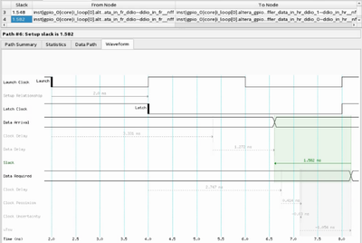
From the HR DDIO IN registers to the FPGA core registers, the data are latched at half-cycle of the launch clock at every 4 ns interval, as shown in the following figure.
Figure 8: Timing Waveform of HR DDIO IN Registers to FPGA Core Registers

This design provides a setup slack of 1.617 ns from HR DDIO IN registers to the FPGA core registers. However, this solution utilizes more resources to implement half-rate data transfer in the design.
6 Summary (Optional)
The following table shows the comparison between the two solutions.
Table 1: Solution Comparison
|
Solution |
Setup Relationship |
Setup Slack |
Timing Path |
Advantages |
|
|
From |
To |
||||
|
Falling edge clock data capturing |
Full cycle latch (4 ns) |
1.814 ns |
DDIO IN pin |
FPGA core register |
• Full rate transfer with maximum operating frequency. • Larger setup slack. • No additional latency. |
|
Half-rate transfer mode |
Half cycle latch (2 ns) |
1.582 ns |
FR DDIO IN pin |
HR DDIO IN registers in Intel FPGA GPIO IP |
• Adequate setup slack. • Larger hold time slack |
|
Half cycle latch (4 ns) |
1.617 ns |
HR DDIO IN registers in Intel FPGA GPIO IP |
FPGA core register |
||
7. Document Revision History
List the revision history for the application note.
|
Date |
Version |
Changes |
|
18 November 2020 |
2020.11.18 |
Initial release |
Community support is provided Monday to Friday. Other contact methods are available here.
Intel does not verify all solutions, including but not limited to any file transfers that may appear in this community. Accordingly, Intel disclaims all express and implied warranties, including without limitation, the implied warranties of merchantability, fitness for a particular purpose, and non-infringement, as well as any warranty arising from course of performance, course of dealing, or usage in trade.
For more complete information about compiler optimizations, see our Optimization Notice.