Generating and Modifying IBIS files for Arria 10 EMIF
Success! Subscription added.
Success! Subscription removed.
Sorry, you must verify to complete this action. Please click the verification link in your email. You may re-send via your profile.
- Intel Community
- Intel Community Knowledge Base
- Product Support Forums Knowledge Base
- FPGA Knowledge Base
- FPGA Wiki
- Generating and Modifying IBIS files for Arria 10 EMIF
Generating and Modifying IBIS files for Arria 10 EMIF
- Subscribe to RSS Feed
- Mark as New
- Mark as Read
- Bookmark
- Subscribe
- Printer Friendly Page
- Report Inappropriate Content
Generating and Modifying IBIS files for Arria 10 EMIF
Generating IBIS files using Quartus
- Create an external memory interface project in Quartus.
- Open the project in Quartus v14.0 or above.
- Select Assignments > Settings.
- On the left panel under Category, select EDA Tool Settings > Board-Level.
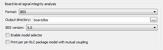
- Under Board-level signal integrity analysis, select the following:

3/3b/Board-level_signal_integrity_analysis_setup .png ( Board-level signal integrity analysis setup.png - click here to view the image )
Board-level signal-integrity analysis setup for IBIS file generation.
After compilation, navigate to the directory where the project is located and open the folder named board. Inside will be another folder labeled ibis, which will contain the generated IBIS file.
Modifying IBIS files for External Memory Interface Simulation
Open your FPGA IBIS model in your favorite text editor.
To change the measurement location from the Pin to the Die
Add the following lines under [Component]:
Si_location Die
Timing_location Die
To change the Voltage Thresholds
This is NOT applicable for DDR4
Find the I/O standard name associated with the DQ net group. For example, for a DDR3 DQ pin with the SSTL 15 I/O standard, you might see something like sstl15_rtnio_g120c_r34c. Find the area where the I/O standard model description is located. Change the Vinl and Vinh values to +/- 70mV of Vref under the Enable Active-Low and [Model Spec] lines.
If Vref = 0.75V, then change the Vinl and Vinh values under the Enable Active-Low line to the following values:
| Vinl | = 0.680 | |
| Vinh | = 0.820 |
And change the Vinh and Vinl values under the [Model Spec] line to the following values:
| Vinh | 0.820 | 0.820 | 0.820 | ||||
| Vinl | 0.680 | 0.680 | 0.680 |
For DDRx Batch Wizard Only
When using the DDRx Batch Simulation Wizard, some warnings may be encountered if the I/O standard name of a given net group (DQ, DQS, or Address/Command/Control) does not match. To address these warnings all the DQ, DM, and Address/Command/Control pins need to have the same model name.
To ensure each net group contains matching model names, make the following changes:
1. Change the model_name for all the DQ, DM, and Address/Command/Control signals from <Interface Standard>_rtnio_<OCT>_<Driver> to
<Interface Standard>_rtpio_<OCT>_<Driver>.
2. Change the model_name for the reset_n signal to match that of the DQ, DM, and Address/Command/Control signals (change the Interface Standard and Differential).
3. Applicable only if you have enabled model selector. The suffixes for every given net group (DQ, DQS, and Address/Command/Control) must be the same. For example, if your DQ0 signal is named pod12_rtpio_g40c_r34cp1_lv_ms8 and DQ1 is named pod12_rtnio_g40c_r34cp1_lv_ms9, make sure that all the DQ pins are named pod12_rtpio_g40c_r34cp1_lv_ms8.
Community support is provided Monday to Friday. Other contact methods are available here.
Intel does not verify all solutions, including but not limited to any file transfers that may appear in this community. Accordingly, Intel disclaims all express and implied warranties, including without limitation, the implied warranties of merchantability, fitness for a particular purpose, and non-infringement, as well as any warranty arising from course of performance, course of dealing, or usage in trade.
For more complete information about compiler optimizations, see our Optimization Notice.