Implementation of Arria 10 ES3 Triple Rate SDI II TX Refclk Switching Feature
Success! Subscription added.
Success! Subscription removed.
Sorry, you must verify to complete this action. Please click the verification link in your email. You may re-send via your profile.
- Intel Community
- Intel Community Knowledge Base
- Product Support Forums Knowledge Base
- FPGA Knowledge Base
- FPGA Wiki
- Implementation of Arria 10 ES3 Triple Rate SDI II TX Refclk Switching Feature
Implementation of Arria 10 ES3 Triple Rate SDI II TX Refclk Switching Feature
- Subscribe to RSS Feed
- Mark as New
- Mark as Read
- Bookmark
- Subscribe
- Printer Friendly Page
- Report Inappropriate Content
Design Overview
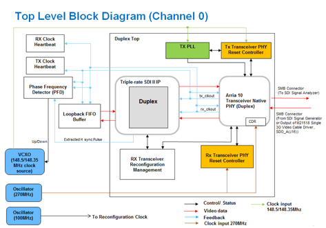
This reference design contains two channels. The instance of SDI II IP in channel 0 is configured to support full duplex and triple rate video standards, SD-SDI, HD-SDI & 3G-SDI. This channel demonstrates the reception & retransmission video data through loopback FIFO buffer.
Channel 1 is configured as the SDI II transmitter IP to support triple rate video standards. This channel demonstrates the implementation of Triple rate SDI II Dynamic TX Clocks Switching Feature where two TX Reference clocks are used to drive the TX PLL to select 1/1.000 or 1/1.001 data rate reconfiguration in SDI II transmitter for Arria ® 10 GX device. Thus, the SDI II transmitter instance can be switched in between 1/1.000 (PAL) or 1/1.001 (NTSC) data rate. The main purpose of this design is to demonstrate the implementation of Tx PLL Reference Clock Switching Feature for fPLL.
a/ae/Top_Level_Block_Diagram_Channel_1.PNG
( Top Level Block Diagram Channel 1.PNG - click here to view image )
System Requirements
This design was compiled in Quartus Prime v16.0.0 b211 for Arria 10 GX PCIe FPGA Development Kit.
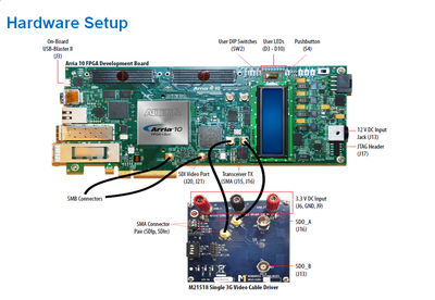
Hardware Setup
( Hardware Setup.PNG - click here to view image )
1. For demonstration on feature of SDI II Tx Dynamic Switching (Channel 1) :
- Power up M21518 single 3G cable driver with 3.3V DC voltage source
- Connect Transceiver Tx(J15,J16) to SMA connector pairs( SDIp,SDIn) of M21518 single 3G cable driver by using SMA cables
2. For the demonstration on SDI II receiver (Channel 0), you can either :
- Connect the transmitter output, SDO_A(J16) of channel 1 to the receiver input, SDI_RX_P(J20) of Channel 0
- Connect an external SDI signal generator to the receiver input, SDI_RX_P(J20) of Channel 0.
Running the Design
1. Set up the hardware as shown at above.
2. Ensure the board setting DIP switches on the development kit are set correctly. Refer to a10-sdi-tx-refclk-dynamic-switching-dipsw-led-pb.docx for more details on this.
3. Download the design file in the link below.
4. Compile the design in Quartus Prime v16.0.0 b211 SJ Standard Edition and configure the .sof file into the Arria 10 GX PCIe FPGA dev kit.
5. For demonstration on feature of SDI II Tx Dynamic Switching (channel 1) :
- Switch DIP switch [SW2.1, SW2.2, SW2.3, SW2.4] to change the internal pattern generator signal standard. Only the following video formats are available for NTSC:
4'b0010 = HD - 1080i60/59.94
4'b0100 = HD - 1080p30/23.96
4'b0101 = HD - 720p60/59.94
4'b0110 = HD - 720p30/29.97
4'b0111 = HD - 1080p30/29.97
4'b1001 = 3Ga - 1080p60/59.94
4'b1011 = 3Gb - 2x1080i60/59.94
4'b1100 = 3Gb - 2x720p30/29.97
4'b1101 = 3Gb - 2x1080p30/29.97
4'b1110 = 3Gb - 1080p60/59.94
- Set up 269.73Mhz for alternative reference clock of fPLL by using Clock Controller Arria10
( Clock Controller.PNG - click here to view image )
- Switch SW2.5 to change the transceiver reference clock.
-0 = select 270Mhz for fPLL to generate 148.5Mhz for A10 Native PHY (for PAL)
-1 = select 269.73Mhz for fPLL to generate 148.35Mhz for A10 Native PHY(for NTSC)
Modifications Steps to use on-board cable driver instead of M21518 Single 3G Video Cable Driver for Channel 1
1. Uncomment this line of code in sdi_tr_a10_txrefclk_switching.v:-
assign sdi_tx_sd_hdn = (ch1_tx_std==2'b00) ? 1'b1 : 1'b0; //This line is needed if use on-board cable driver for channel 1
2. Then, comment this line of code in sdi_tr_a10_txrefclk_switching.v if you are not using on board cable driver for channel 0:-
assign sdi_tx_sd_hdn = (ch0_tx_std==3'b000) ? 1'b1 : 1'b0; //This line is needed if use on-board cable driver for channel 0
3. In assignment editor, change the enabled option for 'sdi_tx_p', ‘sdi_tx_n’, sdi_rx_p' and ‘sdi_rx_n’ pins to "No', For pin 'qsfp_tx_p[0], change the pin location to 'D44'.
4/47/Assignment_editor_CH1.PNG ( Assignment editor CH1.PNG - click here to view image )
- Please refer to the note below for the DIP switch and condition of LEDs:
File:A10 SDI TX refclk dynamic switching DIPSW LED PB.docx
Link to the Design Files
Community support is provided Monday to Friday. Other contact methods are available here.
Intel does not verify all solutions, including but not limited to any file transfers that may appear in this community. Accordingly, Intel disclaims all express and implied warranties, including without limitation, the implied warranties of merchantability, fitness for a particular purpose, and non-infringement, as well as any warranty arising from course of performance, course of dealing, or usage in trade.
For more complete information about compiler optimizations, see our Optimization Notice.

