- Mark as New
- Bookmark
- Subscribe
- Mute
- Subscribe to RSS Feed
- Permalink
- Report Inappropriate Content
Hey there,
I have an FPGA design where a part is running at 150MHz and one part is running with 75MHz (both sourced from the same PLL). So, IMHO the clocks should be synchronous. Of course I need to bring data from one clock domain to another clock domain and I am using a 2FF synchronizer. I already did this also in other designs (eg. MAX10) and AFAIR it worked flawlessly. Now I have a Cyclone IV-FPGA and during synthesis I get a critical warning D101: Data bits are not synchronized when transferred between asynchronous clock domains... My SDC-file has the following entries:set_time_format -unit ns -decimal_places 3
create_clock -name {clk_ext} -period 50.000 -waveform { 0.000 25.000 }
derive_pll_clocks
derive_clock_uncertainty I think everything should work, but it isn't :-/ Has anybody an idea what is going wrong here? Thank you! Regards Mathias
Link Copied
- Mark as New
- Bookmark
- Subscribe
- Mute
- Subscribe to RSS Feed
- Permalink
- Report Inappropriate Content
--- Quote Start --- Hey there, I have an FPGA design where a part is running at 150MHz and one part is running with 75MHz (both sourced from the same PLL). So, IMHO the clocks should be synchronous. Of course I need to bring data from one clock domain to another clock domain and I am using a 2FF synchronizer. I already did this also in other designs (eg. MAX10) and AFAIR it worked flawlessly. Now I have a Cyclone IV-FPGA and during synthesis I get a critical warning D101: Data bits are not synchronized when transferred between asynchronous clock domains... My SDC-file has the following entries:
set_time_format -unit ns -decimal_places 3
create_clock -name {clk_ext} -period 50.000 -waveform { 0.000 25.000 }
derive_pll_clocks
derive_clock_uncertainty
I think everything should work, but it isn't :-/ Has anybody an idea what is going wrong here? Thank you! Regards Mathias --- Quote End --- if clk1 is 150MHz and clk2 is 75MHz and in phase from same PLL then they are related and you don't need synchronisers to cross domains yet you are referring to non related clocks reported so your case is not clear.
- Mark as New
- Bookmark
- Subscribe
- Mute
- Subscribe to RSS Feed
- Permalink
- Report Inappropriate Content
Can you post the clocks report from TimeQuest or the output of write_sdc -expand?
- Mark as New
- Bookmark
- Subscribe
- Mute
- Subscribe to RSS Feed
- Permalink
- Report Inappropriate Content
--- Quote Start --- Can you post the clocks report from TimeQuest or the output of write_sdc -expand? --- Quote End --- Here is the output of the write_sdc -expand command: https://pastebin.com/dhefpn2e AFAIK the negative max input/output delays are to prevent timing errors regarding the input and output pins (the FPGA runs completely asynchronously to the input and output signals).
- Mark as New
- Bookmark
- Subscribe
- Mute
- Subscribe to RSS Feed
- Permalink
- Report Inappropriate Content
--- Quote Start --- if clk1 is 150MHz and clk2 is 75MHz and in phase from same PLL then they are related and you don't need synchronisers to cross domains yet you are referring to non related clocks reported so your case is not clear. --- Quote End --- Yes, they should be related but I do not know why I still get this warning. In the mean time I checked my design on the FPGA and so far it works without problems (I know, that is not a reliable solution...)
- Mark as New
- Bookmark
- Subscribe
- Mute
- Subscribe to RSS Feed
- Permalink
- Report Inappropriate Content
--- Quote Start --- Yes, they should be related but I do not know why I still get this warning. In the mean time I checked my design on the FPGA and so far it works without problems (I know, that is not a reliable solution...) --- Quote End --- My guess is that the warning are not related to PLL clocks but some other clocks in your design
- Mark as New
- Bookmark
- Subscribe
- Mute
- Subscribe to RSS Feed
- Permalink
- Report Inappropriate Content
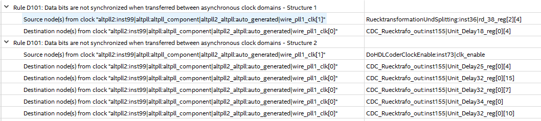
--- Quote Start --- My guess is that the warning are not related to PLL clocks but some other clocks in your design --- Quote End --- To my understanding I have no further clocks beside the two clocks from the PLL and my clk from the external crystal (only used for the PLL). In the compilation report under 'Design Assistant - High Violations' I get a lot of messages (see attachment). In my opinion it is definiteley a problem with the two PLL clocks since the source and destinations nodes are related to the PLL clocks.
- Mark as New
- Bookmark
- Subscribe
- Mute
- Subscribe to RSS Feed
- Permalink
- Report Inappropriate Content
--- Quote Start --- My guess is that the warning are not related to PLL clocks but some other clocks in your design --- Quote End --- To my understanding I have only three clocks: One input clock from an external crystal and used only as PLL input and the two output clocks from the PLL. Looking in the Compilation Report under Design Assistant - High Violations I see that the PLL clocks are the source and the destination of the warnings, see attachment.
- Mark as New
- Bookmark
- Subscribe
- Mute
- Subscribe to RSS Feed
- Permalink
- Report Inappropriate Content
But it reports two PLLs (PLL1 & PLL2)?
- Mark as New
- Bookmark
- Subscribe
- Mute
- Subscribe to RSS Feed
- Permalink
- Report Inappropriate Content
Where do you see this? because of altpll2? I made a new PLL and deleted the old one (altpll1).
- Mark as New
- Bookmark
- Subscribe
- Mute
- Subscribe to RSS Feed
- Permalink
- Report Inappropriate Content
The path name refers to PLL2 then PLL1 and this may give you a clue. Normally all clocks default as related yet your warning is about unrelated clocks. I doubt you have decided on unrelated clocks in your sdc
- Mark as New
- Bookmark
- Subscribe
- Mute
- Subscribe to RSS Feed
- Permalink
- Report Inappropriate Content
I don't know where the *pll1* is coming from, but in the compilation report under Flow Summary Quartus states that 1/4 (25%) of the PLLs are used. I also don't have any command about unrelated clocks in the sdc. You can also have a look at my other post where I did a write_sdc -expand (Result: https://pastebin.com/dhefpn2e)
- Mark as New
- Bookmark
- Subscribe
- Mute
- Subscribe to RSS Feed
- Permalink
- Report Inappropriate Content
--- Quote Start --- I don't know where the *pll1* is coming from, but in the compilation report under Flow Summary Quartus states that 1/4 (25%) of the PLLs are used. I also don't have any command about unrelated clocks in the sdc. You can also have a look at my other post where I did a write_sdc -expand (Result: https://pastebin.com/dhefpn2e) --- Quote End --- It is strange that the tool reports unrelated clocks. Any reason why duty cycle is 50/1 on each clock??
- Mark as New
- Bookmark
- Subscribe
- Mute
- Subscribe to RSS Feed
- Permalink
- Report Inappropriate Content
--- Quote Start --- It is strange that the tool reports unrelated clocks. Any reason why duty cycle is 50/1 on each clock?? --- Quote End --- I don't know, I think this happens due to the write_sdc -expand command. My original SDC-file does not contain these lines (see my first post). But looking in the documentation of SDC Commands (https://www.altera.com/en_us/pdfs/literature/manual/mnl_sdctmq.pdf) at page 2-8: duty_cycle is given in percent, so I think this value corresponds to 50% duty cycle. I think this is OK. Looking in the compilation report states also that the duty cycle is 50.00 for each PLL generated clock. IMHO this is not a problem.
- Mark as New
- Bookmark
- Subscribe
- Mute
- Subscribe to RSS Feed
- Permalink
- Report Inappropriate Content
It is clear that tool regarded clk[0] @150Mhz & clk[1] @75MHz as asynchronous for some reason. It could be they are not in phase or pll mode may be dictating that...
So regard it as asynchronous and then you have to cross domains based on double synchronisers. But you did say you done that, or have you done that properly as the reported paths deny it.- Mark as New
- Bookmark
- Subscribe
- Mute
- Subscribe to RSS Feed
- Permalink
- Report Inappropriate Content
As far as I see I do not have any strange settings in the PLL. I will ignore this warnings and I will see, if my design fails sometime.
Thank you for your ideas and hints :)- Subscribe to RSS Feed
- Mark Topic as New
- Mark Topic as Read
- Float this Topic for Current User
- Bookmark
- Subscribe
- Printer Friendly Page