- Mark as New
- Bookmark
- Subscribe
- Mute
- Subscribe to RSS Feed
- Permalink
- Report Inappropriate Content
Hello,
I have to implement an interface to a sensor chip that delivers its data on several (more than 8) LVDS lines in DDR mode along with an LVDS clock. == Details to the situation == The lines have different phase delays and so I have a hard time to sample all lines correctly. The sensor manufacturer explains the handling in a 2 stage training sequence: * Set the sensor to test mode (where it repeats a static pattern) * first find the right phase for the data bits by shifting the delay until the sampled data changes and take the middle between two setting where it changes * second use bit-slipping until the shiftregisters show the right value The explanation is for Xilinx' Virtex IV devices which seem to have the ability to do the first part without bigger problem - we however are using a Cyclone3 chip and I _have_ bigger problems doing it... == Already thought about == * I've thought about using a separate sample clock for every channel * I would use up at least 2 PLLs for the solution (that I don't have spare...) * If I would use dual clock FiFos to do the clock crossing I would loose the context between the LVDS channels * Timequest can handle input delays but only statically. In the end a delay element with a fixed delay is instantiated. == The real question == I thought, I could implement a structure as in the picture after the diff_input and before the double data rate sampling block. * The single-ended signal is here fed in at four different places * It has to pass either 2 or 4 or 6 or 8 gates * the Delay register which contains only one '1' chooses which path is put out on the output * You could place many more of these and-or structs in if the delay isn't big enough input_delay.gif * Do you think, this could work? * Will the fitter try to make all paths synchronous again - one of the things I fear? * Can I use Timequest to *** make my plans clear (to the fitter)? *** analyse if it works? * The data is coming in with 200MHz DDR - is a little bit logic like some "and"s and "or"s able to insert enough delay for 2.5ns delay (max) Thanks for your patience reading all this. I hope, I haven't forgotten the important parts and you have gotten a clear view of the problem. Since I haven't found any usable information to this topic yet, I'm curious to see if there is a good way of doing this. The sketched solution might be totally bogus - If you feel like it, please tell me so. And if you know a good / better way of realizing an dynamic delay I'm happy to abandon this strange and-or-scheme. Best regards, Roman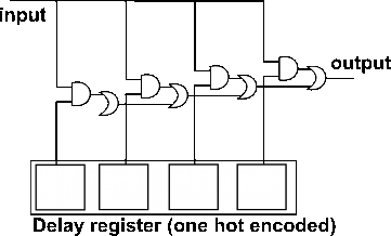
Link Copied
- Mark as New
- Bookmark
- Subscribe
- Mute
- Subscribe to RSS Feed
- Permalink
- Report Inappropriate Content
I don't quite understand you. If you mean you are receiving 8 independant serial DDR channels each with its clock then each channel can be passed to your system clock domain using one dc fifo per channel. Then you can do your bit slipping search.
If your variable delay is due to the board delays then you may get timequest to offset that using static delay per each channel. I don't see why you need dynamic delay if it is board issue. If the sensor data is so variable from source then I will assume each data has its own clock. Your own logic of AND OR is a pitfall I believe.- Mark as New
- Bookmark
- Subscribe
- Mute
- Subscribe to RSS Feed
- Permalink
- Report Inappropriate Content
If you don't have sufficient available PLL outputs in your design, I fear, logic delay chains must be actually considered for the design. It's always an option, if no other solution is available, but I won't expect Timequest being able to calculate a variable delay, as you intend it.
You can expect about 0.2 to 0.25 ns delay per LE (which would represent an AND/OR combination in your schematic), so about 10 LEs and respective control registers would be needed. Because Cyclone III has 4-input LUTs, two selection inputs would be available. Basic ideas about implementation of delay chains can be found in the "Advanced Synthesis Cookbook", the topic has been also discussed at Altera forum, e.g. how to tell the synthesis tool not to remove apparently redundant logic elements. http://www.altera.com/literature/manual/stx_cookbook.pdf- Mark as New
- Bookmark
- Subscribe
- Mute
- Subscribe to RSS Feed
- Permalink
- Report Inappropriate Content
--- Quote Start --- I don't quite understand you. If you mean you are receiving 8 independant serial DDR channels each with its clock I don't see why you need dynamic delay if it is board issue. If the sensor data is so variable from source then I will assume each data has its own clock. Your own logic of AND OR is a pitfall I believe. --- Quote End --- Hi, sadly, I have just one clock and the 8 LVDS channels differ in phase to one another. The delay between the channels is due to the sensor - no board delay and it seems to change over different operating setting (SPI settings inside the sensor) - I have done successfull trainings with one setting while another fails ... The AND OR thing _is_ a pitfall since I have thought about it once more and Input AND (not(DelayReg(0) or DelayReg(1) or DelayReg(2) or DelayReg(3)) would be an equivalent simplification when you "ignored" the timing. => The fitter wouldn't leave anything of it.
- Mark as New
- Bookmark
- Subscribe
- Mute
- Subscribe to RSS Feed
- Permalink
- Report Inappropriate Content
--- Quote Start --- Basic ideas about implementation of delay chains can be found in the "Advanced Synthesis Cookbook", the topic has been also discussed at Altera forum, e.g. how to tell the synthesis tool not to remove apparently redundant logic elements. --- Quote End --- Thanks for this link and a hint that there are people doing such funny stuff... I will take a good look at it and if I get results, I will post them in here. For now, thank's once more... Best regards, Roman
- Mark as New
- Bookmark
- Subscribe
- Mute
- Subscribe to RSS Feed
- Permalink
- Report Inappropriate Content
I forgot to mention, that the LE delay topic is "hidden" in the Random and Pseudorandom Function chapter of the cookbook. It's clear however, that LE delay chains can be made understandable for Quartus through synthesis attributes, and that a range of 2.5 ns is pretty feasible. You can't expect uniform delay steps, because routing delays and the LAB granularity affects the result. Also type variation and temperature dependance of delays should be considered. If your board is facing large temperature changes during operation, a repeated phase calibration may be required.
- Mark as New
- Bookmark
- Subscribe
- Mute
- Subscribe to RSS Feed
- Permalink
- Report Inappropriate Content
--- Quote Start --- I forgot to mention, that the LE delay topic is "hidden" in the Random and Pseudorandom Function chapter of the cookbook. --- Quote End --- Thanks for direction. It had taken me some time to find it but in the end I've gotten there. A first mini-project seemed to show, that the fitter doesn't eat up everything. The magic seems to be a short attribute "syn_keep", which marks the endangered signals. I'll try to integrate the following in my design and see if reality likes it...
library IEEE;
use IEEE.STD_LOGIC_1164.ALL;
use IEEE.STD_LOGIC_ARITH.ALL;
use IEEE.STD_LOGIC_UNSIGNED.ALL;
ENTITY configurable_phase_delay IS GENERIC ( CONF_NR_OF_DELAYS : NATURAL := 32); PORT (
  input     : IN  std_logic;
  output    : OUT std_logic;
  shift_clr : IN  std_logic;
  shift_clk : IN  std_logic;
  shift_up  : IN  std_logic;
  shift_dn  : IN  std_logic
);
END ENTITY;
ARCHITECTURE behav OF configurable_phase_delay IS
SIGNAL delay_register : std_logic_vector(CONF_NR_OF_DELAYS-1 downto 0);
SIGNAL delayed_stages : std_logic_vector(CONF_NR_OF_DELAYS-1 downto 0);
attribute syn_keep: boolean;
attribute syn_keep of delay_register: signal is true;
attribute syn_keep of delayed_stages: signal is true;
BEGIN
output <= delayed_stages(0);
delayed_stages(CONF_NR_OF_DELAYS-1) <= input and delay_register(CONF_NR_OF_DELAYS-1);
delaying : for i in 0 to CONF_NR_OF_DELAYS-2 generate
  delayed_stages(i) <= (input and delay_register(i)) or delayed_stages(i+1);
end generate;
clocking : process(shift_clr, shift_clk) is
begin
  if shift_clr = '1' then
      delay_register   <= (others => '0');
      delay_register(0) <= '1';
  elsif rising_edge(shift_clk) then
    if shift_up = '1' then delay_register <= delay_register(CONF_NR_OF_DELAYS-2 downto 0) & delay_register(CONF_NR_OF_DELAYS-1)          ; end if;
    if shift_dn = '1' then delay_register <= delay_register(0)                            & delay_register(CONF_NR_OF_DELAYS-1 downto 1) ; end if;
  end if;
end process;
END ARCHITECTURE;
- Mark as New
- Bookmark
- Subscribe
- Mute
- Subscribe to RSS Feed
- Permalink
- Report Inappropriate Content
You can see from the post-synthesis netlist, that the LEs are implemented as intended.
- Mark as New
- Bookmark
- Subscribe
- Mute
- Subscribe to RSS Feed
- Permalink
- Report Inappropriate Content
--- Quote Start --- If you don't have sufficient available PLL outputs in your design, I fear, logic delay chains must be actually considered for the design. It's always an option, if no other solution is available, but I won't expect Timequest being able to calculate a variable delay, as you intend it. You can expect about 0.2 to 0.25 ns delay per LE (which would represent an AND/OR combination in your schematic), so about 10 LEs and respective control registers would be needed. Because Cyclone III has 4-input LUTs, two selection inputs would be available. Basic ideas about implementation of delay chains can be found in the "Advanced Synthesis Cookbook", the topic has been also discussed at Altera forum, e.g. how to tell the synthesis tool not to remove apparently redundant logic elements. http://www.altera.com/literature/manual/stx_cookbook.pdf --- Quote End --- Dear FvM: How did you give the value "0.2 to 0.25 ns delay per LE "? Or do you pint me where to find the comments in altera's datasheet?
- Mark as New
- Bookmark
- Subscribe
- Mute
- Subscribe to RSS Feed
- Permalink
- Report Inappropriate Content
I have corrected the delay estimation to 0.3 - 0.4 ns based on tests with Cyclone III. I have previously reported the tests about one year ago at Altera Forum.
- Mark as New
- Bookmark
- Subscribe
- Mute
- Subscribe to RSS Feed
- Permalink
- Report Inappropriate Content
--- Quote Start --- I have corrected the delay estimation to 0.3 - 0.4 ns based on tests with Cyclone III. I have previously reported the tests about one year ago at Altera Forum. --- Quote End --- it seems altera doesn't provide this parameter in their devices' datasheet. i don't find it when try to check all the datasheet.
- Mark as New
- Bookmark
- Subscribe
- Mute
- Subscribe to RSS Feed
- Permalink
- Report Inappropriate Content
I didn't tell about a datasheet parameter. It's a typical and average value, comprised of LUT and routing delay. You'll find individual "micro-timing" parameters in the device handbooks and delay estimation in timing analysis.
But as already stated, the logic cell delay is also depending on PVT variations, a rnage of about 1:2 can be expected. Thus I wonder, what kind of specification you are looking for?- Subscribe to RSS Feed
- Mark Topic as New
- Mark Topic as Read
- Float this Topic for Current User
- Bookmark
- Subscribe
- Printer Friendly Page