- Mark as New
- Bookmark
- Subscribe
- Mute
- Subscribe to RSS Feed
- Permalink
- Report Inappropriate Content
Hi,
I am new to VHDL and am taking this course in my university this semester. I need help with one of the questions from the Laboratory Manual. Students are required to create the following flip-flops (RS, JK, D Flatch, D) using the combination of basic logic gates. Let's pick D Latch, I am sure I can handle the rest by myself. Initially, we were required to create the VHDL code for the basic logic gates (AND, OR, NOT, XOR and so on). This is not an issue. Here is an example for AND gate.
-- VHDL code for AND gate
library ieee;
use ieee.std_logic_1164.all ;
entity andgate is
	port(in1, in2: in std_logic;
		 out1: out std_logic);
end entity andgate;
architecture behavior of andgate is
begin
	out1 <= in1 and in2;
end architecture behavior;
The next part is to create the flip-flops. Now, I am able to create the Block Diagram File (.bdf) for D latch and then convert it to VHDL (File > Create/Update > Create HDL Design File for Current File). However, we are actually required to make use of the logic gates that we have created earlier, so I suspect this must have something to do with using components, port map, etc. I need help with this part. Any help is greatly appreciated, you don't have to post the solution here (I am here to learn not to cheat), just please help me get started in the right direction. Thanks.
Link Copied
5 Replies
- Mark as New
- Bookmark
- Subscribe
- Mute
- Subscribe to RSS Feed
- Permalink
- Report Inappropriate Content
Obviously this is an exercise for ASIC design. To design flips there are several structures.
D flipflops with clear/reset will impress your professor, so I have attached a file. Look at figure 7 I think that structure is easy to implement directly as a set of "NOT AND" of three inputs. I haven't done ASIC and will appreciate your feedback work. May be you will need some delays on the feedback paths...- Mark as New
- Bookmark
- Subscribe
- Mute
- Subscribe to RSS Feed
- Permalink
- Report Inappropriate Content
Hi kaz,
Thanks for your post and the file. I will take a look at it later, then come back with an update.- Mark as New
- Bookmark
- Subscribe
- Mute
- Subscribe to RSS Feed
- Permalink
- Report Inappropriate Content
Hi,
So this is what I have done so far. I referred to this diagram to create the VHDL code for a D latch (D flip flop later). Link: siddiqleksono.files.wordpress.com/2010/10/d-flipflop_284-nand_1-not29.png (I am sorry I can't post clickable links since I am new here, so kindly paste the link above into your browser.) Unfortunately, simulation result yielded both Q and Q_BAR = HIGH. Can anyone please take a look at my code? Thanks! Refer to the attachment for the VHDL code. Edit: I managed to fix the code, refer to the attachment. Now I need help with creating a D flip flop. For D flip flop, I changed ENABLE to CLK. However, I do not know how to proceed from there. Correct me if I am wrong, for D latch, input = output when ENABLE = 1, whereas for D flip flop, input = output when CLK = rising edge.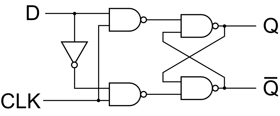
- Mark as New
- Bookmark
- Subscribe
- Mute
- Subscribe to RSS Feed
- Permalink
- Report Inappropriate Content
follow figure 7 of pdf file. I know it does not have enable input. You can leave that for next step. You may for example AND clk and enable but quartus wouldn't be happy as this tool is meant for fpgas and discourages clk gating.
Fig 7 is straighforward set of 6 nand gates each with 3 inputs. Give names to all the nodes and start gating them with not and- Mark as New
- Bookmark
- Subscribe
- Mute
- Subscribe to RSS Feed
- Permalink
- Report Inappropriate Content
Thank you, kaz, I managed to solve the rest, with some help from my university mates.
Reply
Topic Options
- Subscribe to RSS Feed
- Mark Topic as New
- Mark Topic as Read
- Float this Topic for Current User
- Bookmark
- Subscribe
- Printer Friendly Page