We do not receive any response from you to the previous question/reply/answer that I have provided. Please post a response in the next 15 days to allow me to continue to support you. After 15 days, this thread will be transitioned to community support. The community users will be able to help you with your follow-up questions.
- Mark as New
- Bookmark
- Subscribe
- Mute
- Subscribe to RSS Feed
- Permalink
- Report Inappropriate Content
Hi there,
already asked a similar question, but I just can't get a proper answer. Coming from this:
[1] https://forums.intel.com/s/question/0D50P00004NVx2bSAD/how-can-i-use-the-loan-io and this
and many other questions, similar to this one.
What I did so far:
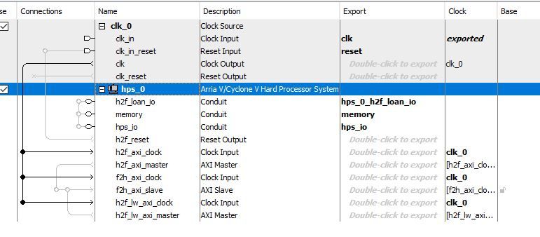
In der Platform Designer I added the HPS
After that I selected the pins 49 and 50 in the table
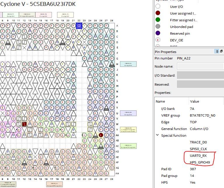
49 and 50 because in the pin planer the pins A22 and B21 are listed as HPS_GPIO 49 and 50
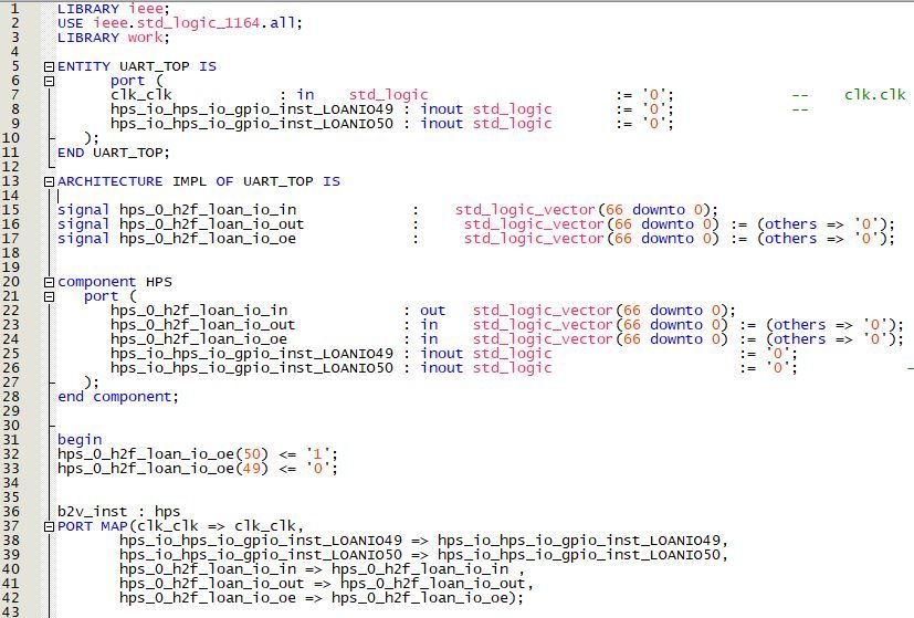
And this is my top entity (I erased all ports and signals for the memory component for better reading)
From [2] I read this:
------------------------------------------
.hps_io_hps_io_gpio_inst_LOANIO20 <-- Connect to top level inout pin .loan_io_in <-- Connect to FPGA
logic .loan_io_out <-- Connect to FPGA
logic .loan_io_oe <-- Connect to FPGA logic
The loan_io_oe controls whether the pin is an output. If '1' at the specified location (in this case loan_io_oe[20] = 1'b1), then it is an output, and you can control the pin writing to loan_io_out[20]. To read an input to the FPGA, just read loan_io_in[20], and set loan_io_oe[20] to 0.
------------------------------------------
This is why I did assignement in line 32 and 33 and I'm not quite sure, if this is right. I connected the hps_io_hps_io_gpio_inst_LOANIO49/50 signals to the top ports and the loan_io_xx to the signals.
And after that I don't know how to continue, because I only try to read and input and give it back so I can read it in the putty terminal. But no matter what I do, it just doesn't work.
Did I do something wrong?
Did I forget something?
Can anyone provide a simple code, how it should be done?
And plz. I am so thankful for your help, but please no refer to any other forum question, document, video, etc. anymore.
In the last couple of days I read so much and watched so many videos but I couldn't find nowhere an explenation how to work with these pins, but dozens of questions regarding this problem.
Thank you !
Link Copied
2 Replies
- Mark as New
- Bookmark
- Subscribe
- Mute
- Subscribe to RSS Feed
- Permalink
- Report Inappropriate Content
Hi
looks like the procedure you followed is right.
instead of connecting to the UART , please connect to another FPGA pin with direction only as out,
From the HPS , toggle the pin and measure from the FPGA side. If you are able to see the toggle ,from the HPS side to FPGA fabric it is connected.
That is how we can check LoanIO function is working. Please let us know the results after trying.
Thanks and Regards
Anil
- Mark as New
- Bookmark
- Subscribe
- Mute
- Subscribe to RSS Feed
- Permalink
- Report Inappropriate Content
Reply
Topic Options
- Subscribe to RSS Feed
- Mark Topic as New
- Mark Topic as Read
- Float this Topic for Current User
- Bookmark
- Subscribe
- Printer Friendly Page


