- Mark as New
- Bookmark
- Subscribe
- Mute
- Subscribe to RSS Feed
- Permalink
- Report Inappropriate Content
Hello,
Im trying to connect ROM with RAM blocks,for this Im write top level entity and connected output of ROM with RAM This is code for ROMLIBRARY ieee; USE ieee.std_logic_1164.all;
use STD.textio.all;
ENTITY sync_rom IS
PORT (
clock: IN std_logic;
address: IN integer range 0 to 511;
data_a_i: OUT integer range 0 to 255;
data_b_q: OUT integer range 0 to 255
);
END sync_rom;
ARCHITECTURE rtl OF sync_rom IS
BEGIN
PROCESS (clock)
BEGIN
IF rising_edge (clock) THEN
CASE address IS
WHEN 0 =>
data_a_i <= 128;
data_b_q <= 128;
WHEN 16 =>
data_a_i <= 128;
data_b_q <= 128;
WHEN 70 =>
data_a_i <= 128;
data_b_q <= 128;
WHEN 400 =>
data_a_i <= 128;
data_b_q <= 128;
WHEN OTHERS =>
data_a_i <= 0;
data_b_q <= 0;
END CASE;
END IF;
END PROCESS;
END rtl;
This is code for RAM library ieee;use ieee.std_logic_1164.all;
use ieee.std_logic_unsigned.all;
entity dp_ram_rbw_scl is
generic (
DATA_WIDTH : integer := 256;
ADDR_WIDTH : integer := 256
);
port (
-- common clock
clk : in std_logic;
-- Port A
we_a : in std_logic;
addr_a : in std_logic_vector(ADDR_WIDTH-1 downto 0);
data_a : in std_logic_vector(DATA_WIDTH-1 downto 0);
q_a : out std_logic_vector(DATA_WIDTH-1 downto 0);
-- Port B
we_b : in std_logic;
addr_b : in std_logic_vector(ADDR_WIDTH-1 downto 0);
data_b : in std_logic_vector(DATA_WIDTH-1 downto 0);
q_b : out std_logic_vector(DATA_WIDTH-1 downto 0)
);
end dp_ram_rbw_scl;
architecture rtl of dp_ram_rbw_scl is
-- Shared memory
type mem_type is array ((2**ADDR_WIDTH)-1 downto 0) of std_logic_vector(DATA_WIDTH-1 downto 0);
shared variable mem : mem_type;
begin
-- Port A
process(clk)
begin
if(clk'event and clk = '1') then
q_a <= mem(conv_integer(addr_a));
if(we_a = '1') then
mem(conv_integer(addr_a)) := data_a;
end if;
end if;
end process;
-- Port B
process(clk)
begin
if(clk'event and clk = '1') then
q_b <= mem(conv_integer(addr_b));
if(we_b = '1') then
mem(conv_integer(addr_b)) := data_b;
end if;
end if;
end process;
end rtl;
after this this I write TOP level entity library ieee;use ieee.std_logic_1164.all;
use ieee.std_logic_unsigned.all;
use ieee.numeric_std.all ;
use ieee.math_real.all ;
use ieee.math_complex.all ;
entity ROMRAM is
port (
clock: IN std_logic;
address: IN integer range 0 to 511;
data_a_i: OUT integer range 0 to 255;
data_b_q: OUT integer range 0 to 255;
DATA_WIDTH : integer := 256;
ADDR_WIDTH : integer := 256;
clk : in std_logic;
we_a : in std_logic;
addr_a : in std_logic_vector(ADDR_WIDTH-1 downto 0);
data_a : in std_logic_vector(DATA_WIDTH-1 downto 0);
q_a : out std_logic_vector(DATA_WIDTH-1 downto 0);
we_b : in std_logic;
addr_b : in std_logic_vector(ADDR_WIDTH-1 downto 0);
data_b : in std_logic_vector(DATA_WIDTH-1 downto 0);
q_b : out std_logic_vector(DATA_WIDTH-1 downto 0);
end ROMRAM;
architecture rtl of ROMRAM is
--- Component decalarartion
Component sync_rom is
port(
clock: IN std_logic;
address: IN integer range 0 to 511;
data_a_i: OUT integer range 0 to 255;
data_b_q: OUT integer range 0 to 255
);
end component;
Component dp_ram_rbw_scl is
generic (
DATA_WIDTH : integer := 256;
ADDR_WIDTH : integer := 256
);
port (
clk : in std_logic;
we_a : in std_logic;
addr_a : in std_logic_vector(DATA_WIDTH-1 downto 0) ;
data_a : in std_logic_vector(DATA_WIDTH-1 downto 0) ;
q_a : out std_logic_vector(DATA_WIDTH-1 downto 0);
we_b : in std_logic;
addr_b : in std_logic_vector(ADDR_WIDTH-1 downto 0) ;
data_b : in std_logic_vector(DATA_WIDTH-1 downto 0) ;
q_b : out std_logic_vector(DATA_WIDTH-1 downto 0)
);
end component;
for all : sync_rom use entity work.sync_rom(rtl);
--for all : dp_ram_rbw_scl use entity work.dp_ram_rbw_scl(rtl);
--Signal data_a_i: integer range 0 to 255;
--data_b_q_a: std_logic_vector(255 downto 0);--interanal signals
begin
--inst : dp_ram_rbw_scl port map ( addr_a=> addr_a,
--clk=> clk,we_a=>we_a,data_a=>data_a,addr_b=>addr_b,data_b=>data_b,we_b=>we_b);
q_a<= addr_a and data_a;
-- Component Instantiation
C1: sync_rom Port map (
clock => clock,
address =>address,
data_a_i =>data_a_i,
data_b_q =>data_b_q
);
C2: dp_ram_rbw_scl Port map (
clk=>clk,
we_a=>we_a,
addr_a=>addr_a,
data_a =>data_a,
q_a=>q_a,
we_b=>we_b,
addr_b=>addr_b,
data_b =>data_b,
q_b=>q_b
);
data_a_i<=to_integer ( unsigned (data_a));
data_b_q<=to_integer ( unsigned (data_b));
end rtl;
But this code doesnt work/Could you please give me some hints for solution? I want to connect data_a_i(ROM) with data_a(RAM) and data_b_q(ROM) with data_b(RAM) I get next errors Error (10346): VHDL error at Vhdl2.vhd(70): formal port or parameter "addr_a" must have actual or default value Error (10346): VHDL error at Vhdl2.vhd(70): formal port or parameter "data_a" must have actual or default value Error (10346): VHDL error at Vhdl2.vhd(70): formal port or parameter "addr_b" must have actual or default value Error (10346): VHDL error at Vhdl2.vhd(70): formal port or parameter "data_b" must have actual or default value
Link Copied
- « Previous
-
- 1
- 2
- Next »
- Mark as New
- Bookmark
- Subscribe
- Mute
- Subscribe to RSS Feed
- Permalink
- Report Inappropriate Content
I want that my datawidth should be 256
I have a question,data_a and data_a_i should be connected,so this mean that those signals should be internal,and we dont need to declare it in TOP level entity.Am I right?- Mark as New
- Bookmark
- Subscribe
- Mute
- Subscribe to RSS Feed
- Permalink
- Report Inappropriate Content
--- Quote Start --- I want that my datawidth should be 256 --- Quote End --- why, 256 bits address requires memory size of 2^256 an that is nearly equal to all Universe rams put together??
- Mark as New
- Bookmark
- Subscribe
- Mute
- Subscribe to RSS Feed
- Permalink
- Report Inappropriate Content
yes,now its working,but i dont see connection between data_a_i and data_a, data_b_q and data_b)sorry my bad.yes i need just 8.but what about,data_a and data_a_i should be connected,so this mean that those signals should be internal,and we dont need to declare it in TOP level entity.Am I right?
- Mark as New
- Bookmark
- Subscribe
- Mute
- Subscribe to RSS Feed
- Permalink
- Report Inappropriate Content
--- Quote Start --- yes)sorry my bad.yes i need just 8.but what about,data_a and data_a_i should be connected,so this mean that those signals should be internal,and we dont need to declare it in TOP level entity.Am I right? --- Quote End --- The role is this: any node used at top level should be declared either as port or internal signal then connected to lower level interface signals
- Mark as New
- Bookmark
- Subscribe
- Mute
- Subscribe to RSS Feed
- Permalink
- Report Inappropriate Content
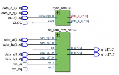
yes,now its working,but i dont see connection in RTL viewer between data_a_i and data_a, data_b_q and data_b)
library ieee;     use ieee.std_logic_1164.all;
     use ieee.std_logic_unsigned.all;
      use ieee.std_logic_signed.all;
    use ieee.numeric_std.all ;
    use ieee.math_real.all ;
    use ieee.math_complex.all ;
entity ROMRAM is
generic(
          DATA_WIDTHi : integer := 8;
        ADDR_WIDTHi : integer := 8);
    port (
        CLOC: IN std_logic;
        ADD: IN integer range 0 to 511;
          data_a : in std_logic_vector(DATA_WIDTHi-1 downto 0);
          data_b : in std_logic_vector(DATA_WIDTHi-1 downto 0);
        data_a_i : in integer range 0 to 255;
          data_b_q : in integer range 0 to 255;
        --clk    : in  std_logic;
        we_ai   : in  std_logic;
        addr_ai : in  std_logic_vector(ADDR_WIDTHi-1 downto 0);
        q_ai   : out std_logic_vector(DATA_WIDTHi-1 downto 0);
        we_bq   : in  std_logic;
        addr_bq : in  std_logic_vector(ADDR_WIDTHi-1 downto 0);
        q_bq    : out std_logic_vector(DATA_WIDTHi-1 downto 0));
end ROMRAM;
architecture rtl of ROMRAM is
--- Component decalarartion
Component sync_rom is
    port(
        clock: IN std_logic;
        address: IN integer range 0 to 511;
        data_a_i: OUT integer range 0 to 255;
        data_b_q: OUT integer range 0 to 255
        );
end component;

Component dp_ram_rbw_scl is
generic (
        DATA_WIDTH : integer := 8;
        ADDR_WIDTH : integer := 8
            );
    port(
        clk    : in  std_logic;
        we_a   : in  std_logic;
        addr_a : in  std_logic_vector(ADDR_WIDTH-1 downto 0) ;
        data_a : in  std_logic_vector(DATA_WIDTH-1 downto 0) ;
        q_a    : out std_logic_vector(DATA_WIDTH-1 downto 0);
        we_b   : in  std_logic;
        addr_b : in  std_logic_vector(ADDR_WIDTH-1 downto 0) ;
        data_b : in  std_logic_vector(DATA_WIDTH-1 downto 0) ;
        q_b    : out std_logic_vector(DATA_WIDTH-1 downto 0)
        );
end component;
for all : sync_rom use entity work.sync_rom(rtl);
for all : dp_ram_rbw_scl use entity work.dp_ram_rbw_scl(rtl);
Signal     data_a_i_i: integer range 0 to 255;--interanal signals
Signal     data_b_q_i: integer range 0 to 255;--interanal signals
begin
-- Component Instantiation
C1: sync_rom Port map (
                                clock => CLOC,
                                address =>ADD,
                                data_a_i =>data_a_i_i,
                                data_b_q =>data_b_q_i
                                );
C2: dp_ram_rbw_scl
Port map (
                                    clk=>CLOC,
                                    we_a=>we_ai,
                                    addr_a=>addr_ai,
                                    data_a =>data_a,
                                    q_a=>q_ai,
                                    we_b=>we_bq,
                                    addr_b=>addr_bq,
                                    data_b =>data_b,
                                    q_b=>q_bq
                                );
                                            data_a_i_i<= to_integer(unsigned(data_a));
                                            data_b_q_i<= to_integer(unsigned(data_b));
end rtl;
- Mark as New
- Bookmark
- Subscribe
- Mute
- Subscribe to RSS Feed
- Permalink
- Report Inappropriate Content
if it is only type conversion then that is done at compile time and no logic is involved in fpga. Similarly any direct wiring
- Mark as New
- Bookmark
- Subscribe
- Mute
- Subscribe to RSS Feed
- Permalink
- Report Inappropriate Content
also do not mix all those libraries. Use only numeric_std for type conversion.
with some tools they allow direct type conversion on the port map- Mark as New
- Bookmark
- Subscribe
- Mute
- Subscribe to RSS Feed
- Permalink
- Report Inappropriate Content
ok,so as I understood,I made only conversion and no logic involved in FPGA,so i didnt connect those data_.... ports?
- Mark as New
- Bookmark
- Subscribe
- Mute
- Subscribe to RSS Feed
- Permalink
- Report Inappropriate Content
--- Quote Start --- ok,so as I understood,I made only conversion and no logic involved in FPGA,so i didnt connect those data_.... ports? --- Quote End --- you wired them but after conversion so that signal types match and tool does not reject it.
- Mark as New
- Bookmark
- Subscribe
- Mute
- Subscribe to RSS Feed
- Permalink
- Report Inappropriate Content
thanks a lot for help))as I understood this code is working properly?
- Mark as New
- Bookmark
- Subscribe
- Mute
- Subscribe to RSS Feed
- Permalink
- Report Inappropriate Content
rom does not need data input or write. ram needs them so check your wiring again.
- Mark as New
- Bookmark
- Subscribe
- Mute
- Subscribe to RSS Feed
- Permalink
- Report Inappropriate Content
For RAM,I need to connect addr_a _b ports?with adddress port from ROM?and data_a and data_b?
- Mark as New
- Bookmark
- Subscribe
- Mute
- Subscribe to RSS Feed
- Permalink
- Report Inappropriate Content
now, I competed this code
library ieee;
     use ieee.std_logic_1164.all;
     use ieee.numeric_std.all ;
entity ROMRAM is
generic(
		  DATA_WIDTHi : integer := 8;
        ADDR_WIDTHi : integer := 8);
    port (
        CLOC: IN std_logic;
        ADD: IN integer range 0 to 511;
		  --data_a : in std_logic_vector(DATA_WIDTHi-1 downto 0);
		  --data_b : in std_logic_vector(DATA_WIDTHi-1 downto 0);
        --data_a_i : out integer range 0 to 255;
		  --data_b_q : out integer range 0 to 255;
        --clk    : in  std_logic;
        we_ai   : in  std_logic;
        addr_ai : in  std_logic_vector(ADDR_WIDTHi-1 downto 0);
        q_ai   : out std_logic_vector(DATA_WIDTHi-1 downto 0);
        we_bq   : in  std_logic;
        addr_bq : in  std_logic_vector(ADDR_WIDTHi-1 downto 0);
        q_bq    : out std_logic_vector(DATA_WIDTHi-1 downto 0));
end ROMRAM;
architecture rtl of ROMRAM is
--- Component decalarartion
Component sync_rom is
    port(
        clock: IN std_logic;
        address: IN integer range 0 to 511;
        data_a_i: OUT integer range 0 to 255;
        data_b_q: OUT integer range 0 to 255
        );
end component;

Component dp_ram_rbw_scl is
generic (
        DATA_WIDTH : integer := 8;
        ADDR_WIDTH : integer := 8
            );
    port(
        clk    : in  std_logic;
        we_a   : in  std_logic;
        addr_a : in  std_logic_vector(ADDR_WIDTH-1 downto 0) ;
        data_a : in  std_logic_vector(DATA_WIDTH-1 downto 0) ;
        q_a    : out std_logic_vector(DATA_WIDTH-1 downto 0);
        we_b   : in  std_logic;
        addr_b : in  std_logic_vector(ADDR_WIDTH-1 downto 0) ;
        data_b : in  std_logic_vector(DATA_WIDTH-1 downto 0) ;
        q_b    : out std_logic_vector(DATA_WIDTH-1 downto 0)
        );
end component;
for all : sync_rom use entity work.sync_rom(rtl);
for all : dp_ram_rbw_scl use entity work.dp_ram_rbw_scl(rtl);
Signal     data_a_i_i: integer range 0 to 255;--interanal signals
signal dt_ai: std_logic_vector(7 downto 0);
Signal     data_b_q_i: integer range 0 to 255;--interanal signals
signal dt_bq: std_logic_vector(7 downto 0);
begin
-- Component Instantiation
C1: sync_rom Port map (
                                clock => CLOC,
                                address =>ADD,
                                data_a_i =>data_a_i_i,
                                data_b_q =>data_b_q_i
                                );
C2: dp_ram_rbw_scl
Port map (
                                    clk=>CLOC,
                                    we_a=>we_ai,
                                    addr_a=>addr_ai,
                                    data_a =>dt_ai,
                                    q_a=>q_ai,
                                    we_b=>we_bq,
                                    addr_b=>addr_bq,
                                    data_b =>dt_bq,
                                    q_b=>q_bq
                                );
										  dt_ai<=std_logic_vector(to_unsigned(data_a_i_i,dt_ai'length));
										  dt_bq<=std_logic_vector(to_unsigned(data_b_q_i,dt_bq'length));
											--data_a_i<= to_integer(unsigned(data_a));
											--data_b_q<= to_integer(unsigned(data_b));
											--data_a_i <= std_logic_vector(to_unsigned(data_a_i,data_a'length));
											--data_a=> data_a_i_i
end rtl;
- Mark as New
- Bookmark
- Subscribe
- Mute
- Subscribe to RSS Feed
- Permalink
- Report Inappropriate Content
how is it looks now?
- Mark as New
- Bookmark
- Subscribe
- Mute
- Subscribe to RSS Feed
- Permalink
- Report Inappropriate Content
--- Quote Start --- how is it looks now? --- Quote End --- code ok but overall idea unclear. What do you put in rom (with dual port output). You then address rom from outside and address ram from outside. What is the purpose. I also suggest (strongly) changing the name cloc to clock or clk just for consistency. check your rom code address range(now 0~255).
- Mark as New
- Bookmark
- Subscribe
- Mute
- Subscribe to RSS Feed
- Permalink
- Report Inappropriate Content
After this I want to add this block in fft_engine(http://opencores.org/project,versatile_fft)
In ROM when fft see the next add like 0,16,70,400 in this addresses we put 128 values,for other we put just 0 Data from ROM should go to the RAM- Mark as New
- Bookmark
- Subscribe
- Mute
- Subscribe to RSS Feed
- Permalink
- Report Inappropriate Content
--- Quote Start --- After this I want to add this block in fft_engine(http://opencores.org/project,versatile_fft) In ROM when fft see the next add like 0,16,70,400 in this addresses we put 128 values,for other we put just 0 Data from ROM should go to the RAM --- Quote End --- But I expect a proper fft core to require just input stream +plus start of frame/end of frame etc. So why do you care about addressing issues you mentioned
- Subscribe to RSS Feed
- Mark Topic as New
- Mark Topic as Read
- Float this Topic for Current User
- Bookmark
- Subscribe
- Printer Friendly Page
- « Previous
-
- 1
- 2
- Next »