- Mark as New
- Bookmark
- Subscribe
- Mute
- Subscribe to RSS Feed
- Permalink
- Report Inappropriate Content
Hy everyone..
I have a system of SOPC here (attached* pic1). I access my SOPC using NIOS II IDE,by using a simple read/write function through it.(*attached pic2) my objective here is to monitor the input and output pin to and from SDRAM(which is sdram.v file for SOPC builder), that's why I'm using the Signal Tap II Logic Analyzer. I am following below instruction to create and use this function: http://www.altera.com/literature/an/an323.pdf (I'll call Signal Tap II as STII later) The step stuck on the "create a new signaltap ii file and add signals to monitor" step (2f). This is the step to find the clock of my system. Since i can't find any nodes when my filter setting was set to "all" , so I changed the filter to signaltapii: pre-syntesis and I got pic3(*attached pic3). From Pic1, I am assuming that my CPU clock is attached to on pll.c0, so I pick c0 as my system clock on the STII. I add all of the input and output signal from sdram.v to the function and I got pic4. When I run this setting together with NIOS II, I got the result but it runs so fast that I can't see the changes I want to see. I was expecting that the input address of the SDRAM will change (maybe some kind of 00_0032h)and the data will change too(maybe some kind of 0000_0032h). I have try to trigger the falue of az_addr (which is maybe the address signal of SDRAM) to 00_0032h (attached pic4), but I cant see the expected result. i am xpecting the result like the waveform on the modelsim or quartus waveform which can be dragged left and right to see the changing of the monitored signal. is it possible? Thank you in advance Yuyex :oLink Copied
- Mark as New
- Bookmark
- Subscribe
- Mute
- Subscribe to RSS Feed
- Permalink
- Report Inappropriate Content
- Mark as New
- Bookmark
- Subscribe
- Mute
- Subscribe to RSS Feed
- Permalink
- Report Inappropriate Content
--- Quote Start --- Hy everyone.. I have a system of SOPC here (attached* pic1). I access my SOPC using NIOS II IDE,by using a simple read/write function through it.(*attached pic2) my objective here is to monitor the input and output pin to and from SDRAM(which is sdram.v file for SOPC builder), that's why I'm using the Signal Tap II Logic Analyzer. I am following below instruction to create and use this function: http://www.altera.com/literature/an/an323.pdf (I'll call Signal Tap II as STII later) The step stuck on the "create a new signaltap ii file and add signals to monitor" step (2f). This is the step to find the clock of my system. Since i can't find any nodes when my filter setting was set to "all" , so I changed the filter to signaltapii: pre-syntesis and I got pic3(*attached pic3). From Pic1, I am assuming that my CPU clock is attached to on pll.c0, so I pick c0 as my system clock on the STII. I add all of the input and output signal from sdram.v to the function and I got pic4. When I run this setting together with NIOS II, I got the result but it runs so fast that I can't see the changes I want to see. I was expecting that the input address of the SDRAM will change (maybe some kind of 00_0032h)and the data will change too(maybe some kind of 0000_0032h). I have try to trigger the falue of az_addr (which is maybe the address signal of SDRAM) to 00_0032h (attached pic4), but I cant see the expected result. i am xpecting the result like the waveform on the modelsim or quartus waveform which can be dragged left and right to see the changing of the monitored signal. is it possible? Thank you in advance Yuyex :o --- Quote End --- The Nios is also running in SDRAM? Then where are reset and exception vectors placed? Are You writing to those addresses? Anyway, if Nios is also running on SDRAM, then You see Nios CPU writing/reading the memory. If You need to trigger to exact place, then place trigger on required signal. --- Quote Start --- Result of TMII (pic5) I am also wondering why my sdram_clk isnt "clicking" Thank you :o --- Quote End --- The SignalTap LA is fully synchronous. Every rising edge You sample a signal, that is the clock itself, so what do You expect?
- Mark as New
- Bookmark
- Subscribe
- Mute
- Subscribe to RSS Feed
- Permalink
- Report Inappropriate Content
As I've mentioned before: Nios CPU also does read and write to the memory, that's why You see address changes. Better add on-chip RAM to the SOPC and do tests there. Safe and clear how it works.
For the LA You have shifted clock by -65deg for sdram chip. How can You expect to see this clock signal if every rising edge of the LA clock samples SDRAM clock at the same place? E.g. 1) SDRAM chip clk (shifted by -65deg) 2) LA sampling clock
__|--|__|--|__
___|--|__|--|__
At every rising edge of the signal (2) it samples signal (1) and the sample is always at value '1'.
- Mark as New
- Bookmark
- Subscribe
- Mute
- Subscribe to RSS Feed
- Permalink
- Report Inappropriate Content
--- Quote Start --- As I've mentioned before: Nios CPU also does read and write to the memory, that's why You see address changes. --- Quote End --- Ah .. I got it .. the memory address is keep on changing since CPU have to compile the instruction to the on-chip ram. Thank you for the guide on this :o --- Quote Start --- Better add on-chip RAM to the SOPC and do tests there. Safe and clear how it works. --- Quote End --- I added on-chip memory with another specific purpose. I am using SDRAM because my project is to improve the performance of SDRAM controller. Thank you for the advice though. QUOTE=Socrates;142581] For the LA You have shifted clock by -65deg for sdram chip. How can You expect to see this clock signal if every rising edge of the LA clock samples SDRAM clock at the same place? E.g. 1) SDRAM chip clk (shifted by -65deg) 2) LA sampling clock
__|--|__|--|__
___|--|__|--|__
At every rising edge of the signal (2) it samples signal (1) and the sample is always at value '1'. --- Quote End --- Ah~ I got what you mean.. Thank you so much, Socrates :o Btw is there any method to see the "whole waveform action" without using trigger event, although I find it useful enough. Just wondering. Thank you in advance Yuyex:o
- Mark as New
- Bookmark
- Subscribe
- Mute
- Subscribe to RSS Feed
- Permalink
- Report Inappropriate Content
You want to see the clock? Then use at least double sampling freq., but it has to be phase locked, so use the same PLL. Anyway, I don't see why this would be useful...
- Mark as New
- Bookmark
- Subscribe
- Mute
- Subscribe to RSS Feed
- Permalink
- Report Inappropriate Content
--- Quote Start --- You want to see the clock? Then use at least double sampling freq., but it has to be phase locked, so use the same PLL. Anyway, I don't see why this would be useful... --- Quote End --- Yup .. I got it , Socrates.. Thank you very much :))
- Mark as New
- Bookmark
- Subscribe
- Mute
- Subscribe to RSS Feed
- Permalink
- Report Inappropriate Content
I got a problem.. I write and read to 10 address of SDRAM (address:00_0000h~00_0009h) (data : 0~9). (*attached)
I set the trigger event on the Rising Edge of az_cs (chip select) since it'll work on the read/write request from CPU. (*attached) But the result in LA only run for 6 rising edge of az_cs.(*attached) Can anyone tell me how to run the whole waveform until all of the az_cs wont rise? Thank you in advance Yuyex:o- Mark as New
- Bookmark
- Subscribe
- Mute
- Subscribe to RSS Feed
- Permalink
- Report Inappropriate Content
Do You see that You're writing to address, where Your Nios CPU firmware is palced? you're basically destroying the CPU itself. You are probably writing to the reset vector, so the CPU resets and SDRAM controller resets too.
- Mark as New
- Bookmark
- Subscribe
- Mute
- Subscribe to RSS Feed
- Permalink
- Report Inappropriate Content
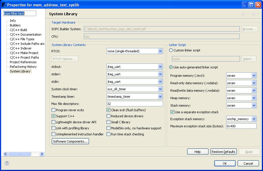
--- Quote Start --- Do You see that You're writing to address, where Your Nios CPU firmware is palced? you're basically destroying the CPU itself. You are probably writing to the reset vector, so the CPU resets and SDRAM controller resets too. --- Quote End --- Hy Socrates.. You mean this reset vector??(attached*) I didn't write to that address, did I ? I write the data to SDRAM_BASE .. Please correct me if I am wrong .. Or maybe you can show me some example? Thank you in advance Yuyex:o
- Mark as New
- Bookmark
- Subscribe
- Mute
- Subscribe to RSS Feed
- Permalink
- Report Inappropriate Content
Oh, then it's ok. Where are .heap, .bss and other stuff placed?
- Mark as New
- Bookmark
- Subscribe
- Mute
- Subscribe to RSS Feed
- Permalink
- Report Inappropriate Content
- Mark as New
- Bookmark
- Subscribe
- Mute
- Subscribe to RSS Feed
- Permalink
- Report Inappropriate Content
I have get the way to increase the sampling data .. Just increase the value on the sample depth .. (*attached)
But is there anyone who can help me, why is my az_cs is rising only 3 times meanwhile I expected it to rise 4 times (2 for write and 2 for read). My NIOS application (*attached) Thank you in advance Yuyex:o- Subscribe to RSS Feed
- Mark Topic as New
- Mark Topic as Read
- Float this Topic for Current User
- Bookmark
- Subscribe
- Printer Friendly Page