- Mark as New
- Bookmark
- Subscribe
- Mute
- Subscribe to RSS Feed
- Permalink
- Report Inappropriate Content
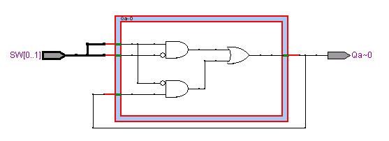
Sorry, found what I had missed: There *was* a gnarly inverter on the output of the latch, should have picked up on the Qa~0 name. Would have deleted the post again but that doesn't seem to be an option..
Hi, not sure where to report this, so I figured I'd go with the Quartus forum. I'm simply walking through the DE1 labs and noticed that the circuit drawn by the Technology Map Viewer (Post-Mapping) looks wrong for the following piece of code:
module D_latch(clk,D,Q);
input clk, D;
output Q;
wire S, R, S_g, R_g, Qa, Qb;
assign R   = ~D;
assign S_g = ~(D & clk);
assign R_g = ~(R & clk);
assign Qa  = ~(S_g & Qb);
assign Qb  = ~(R_g & Qa);
assign Q   = Qa;
endmodule
I get the attached diagram, no inverters outside - what's the inverter doing on the upper and gate? Synthesized design works as expected, RTL Viewer looks good, too. I must have missed something, but what?
Link Copied
0 Replies
Reply
Topic Options
- Subscribe to RSS Feed
- Mark Topic as New
- Mark Topic as Read
- Float this Topic for Current User
- Bookmark
- Subscribe
- Printer Friendly Page