- Mark as New
- Bookmark
- Subscribe
- Mute
- Subscribe to RSS Feed
- Permalink
- Report Inappropriate Content
Hello,
Probably I didn't properly define timing constraints ... TimeQuest reported quite a lot of timing violations. In this connection I have one question - does exist some straightforward approach on working around "timing violations" ? For example on the image below there are 2 screenshots form TimeQuest:- top screenshot - results of "Report Top Failing Paths"
- bottom screenshot - "Peport Timing" for the path, highlighted in yellow on the top screenshot
.jpg)
Link Copied
- Mark as New
- Bookmark
- Subscribe
- Mute
- Subscribe to RSS Feed
- Permalink
- Report Inappropriate Content
Multi cycle path is only an option if it really is a true multicycle path. Eg. From register to register that use the same periodic enable.
If multi cycle is not an option, the easiest fix is modifying the code to increase the pipelining the design.- Mark as New
- Bookmark
- Subscribe
- Mute
- Subscribe to RSS Feed
- Permalink
- Report Inappropriate Content
--- Quote Start --- Multi cycle path is only an option if it really is a true multicycle path. Eg. From register to register that use the same periodic enable. If multi cycle is not an option, the easiest fix is modifying the code to increase the pipelining the design. --- Quote End --- Can I make a conclusion from the left part of the bottom screenshot (i.e. waveform) that the only option is multicycle: lookeng at the image we can state that shifting forward latch edge by 1 cycle should resolve the problem, isn't it ? Concerning modifying the code, the code is very simple: it consists of instantiating of Qsys module (I put it below) ... or you mean modify Qsys ? By the way, I've tried multicycle option with following commands in .SDC file: set_multicycle_path -setup -to [get_nodes {nios_led2_sdram:u0|nios_led2_sdram_sdram:sdram|za_data[*]}] 2 set_multicycle_path -hold -to [get_nodes {nios_led2_sdram:u0|nios_led2_sdram_sdram:sdram|za_data[*]}] 1 Unfortunately they wasn't taken into account. Here is fragment of TimeQuest output: Ignored set_multicycle_path at SDC1.sdc(30): Argument <to> is a collection that is not of clk, kpr, reg, port, pin, cell or partition type set_multicycle_path -setup -to [get_nodes {nios_led2_sdram:u0|nios_led2_sdram_sdram:sdram|za_data[*]}] 2 Ignored set_multicycle_path at SDC1.sdc(31): Argument <to> is a collection that is not of clk, kpr, reg, port, pin, cell or partition type set_multicycle_path -hold -to [get_nodes {nios_led2_sdram:u0|nios_led2_sdram_sdram:sdram|za_data[*]}] 1 Here is top module: module nios_led2_top (input clk, input [9:0] sw, input [3:0] key, output[4:0] led_H, led_L, output [6:0] hex3, hex2 , hex1, hex0, output [12:0] sdram_addr, inout [15:0] sdram_dq, output [1:0] sdram_bank, output sdram_cas_n, sdram_ras_n, sdram_cke, sdram_cs_n, sdram_clk, output sdram_dqmh, sdram_dqml, sdram_we_n); wire [31:0] sseg; assign hex3 = sseg[31:24]; assign hex2 = sseg[22:16]; assign hex1 = sseg[14:8]; assign hex0 = sseg[6:0]; nios_led2_sdram u0 ( .btn_export (key), .clk_clk (clk), .led_h_export (led_H), .led_l_export (led_L), .reset_reset_n (1'b1), .sdram_wire_addr (sdram_addr), .sdram_wire_ba (sdram_bank), .sdram_wire_cas_n (sdram_cas_n), .sdram_wire_cke (sdram_cke), .sdram_wire_cs_n (sdram_cs_n), .sdram_wire_dq (sdram_dq), .sdram_wire_dqm ({sdram_dqmh, sdram_dqml}), .sdram_wire_ras_n (sdram_ras_n), .sdram_wire_we_n (sdram_we_n), .sseg_export (sseg), .switch_export (sw), .clk_sdram_clk (sdram_clk) ); // nios_led2_nopll u0 ( // .btn_export (key), // btn.export // .clk_clk (clk), // clk.clk // .led_h_export (led_H), // led_h.export // .led_l_export (led_L), // led_l.export // .reset_reset_n (1'b1), // reset.reset_n // .sseg_export (sseg), // sseg.export // .switch_export (sw) // switch.export // ); endmodule
- Mark as New
- Bookmark
- Subscribe
- Mute
- Subscribe to RSS Feed
- Permalink
- Report Inappropriate Content
--- Quote Start --- Probably I didn't properly define timing constraints ... TimeQuest reported quite a lot of timing violations. --- Quote End --- 1. Check if there are any ignored constrains. 2. Check if there are any unconstrained paths. 3. Check clock transfers and make sure that there are no invalid clock transfers analysed. --- Quote Start --- Does exist some straightforward approach on working around "timing violations" ? --- Quote End --- It depends what causes those timing violations. Violations between unrelated clocks or paths - usually can be solved by setting clock groups or setting false path between unrelated paths. Violations in register-to-register level - usually caused by bad coding style, go back to your VHDL/Verilog code and fix it. Violations in I/O - can be solved by using PLL and clock phase shift, clock inversion ect.
- Mark as New
- Bookmark
- Subscribe
- Mute
- Subscribe to RSS Feed
- Permalink
- Report Inappropriate Content
First, short remark concerning forum policy ... quite frequently a posted message doesn't appear immediately, but is retained for approval.
And this approval can be as long as ... 24h. I asked for this issue to forum administration, but still didn't receive any answer. It occurred once more time yesterday: I answered to Tricky, but my message is still "in approval". Well let's return to subject ... --- Quote Start --- 1. Check if there are any ignored constrains. --- Quote End --- Yes, there are 2 ignored constraints (as I've already exposed yesterday in my non-posted message). Trying to resolve the violations issues on sdram data bus (blue cadre on the screenshot in 1st message), I was thinking (probably wrongly) that the best solution here is to introduce multicycles, i.e. "open the window", using terminology of the ryan scoville's timequest user guide (at least as I understood it). Looking at the Waveform diagram in "Timing Report" for SDRAM data [6] (left part of bottom screenshot in the 1st message), one can believe that problem can be fixed by shifting forward the "latch edge". That is what I tried to do with the following commands: set_multicycle_path -setup -to [get_nodes {nios_led2_sdram:u0|nios_led2_sdram_sdram:sdram|za_data[*]}] 2 set_multicycle_path -hold -to [get_nodes {nios_led2_sdram:u0|nios_led2_sdram_sdram:sdram|za_data[*]}] 1 And these commands were ignored by TimeQuest parser. --- Quote Start --- 2. Check if there are any unconstrained paths. --- Quote End --- No, after applying your suggestions (in another thread), there is no more unconstrained paths --- Quote Start --- 3. Check clock transfers and make sure that there are no invalid clock transfers analysed. --- Quote End --- At 1st glance NO ... at least there is nothing "in red" --- Quote Start --- Violations between unrelated clocks or paths - usually can be solved by setting clock groups or setting false path between unrelated paths. Violations in register-to-register level - usually caused by bad coding style, go back to your VHDL/Verilog code and fix it. Violations in I/O - can be solved by using PLL and clock phase shift, clock inversion ect. --- Quote End --- In my simple case there are only a few clocks: external clock, 2 PLL generated clocks and JTAG clock - altera_reserved_tck. Concerning coding style - actually there is no code, only Qsys module instantiation. So, perhaps, my case correspond to "Violations in I/O" ? Here I have 2 questions:- The PLL module in Qsys has 2 ouput and one of them is phase-shifted. This phase shift isn't reflected in .SDC file ... I beleived that TimeQuest can handle this shift without .SDC modification (again probably I'm wrong)
- So even in this case multicycles can't be considered as "reliable remedy"
- Mark as New
- Bookmark
- Subscribe
- Mute
- Subscribe to RSS Feed
- Permalink
- Report Inappropriate Content
--- Quote Start --- The PLL module in Qsys has 2 ouput and one of them is phase-shifted. This phase shift isn't reflected in .SDC file ... I beleived that TimeQuest can handle this shift without .SDC modification (again probably I'm wrong) --- Quote End --- Yes, if you use derive_pll_clocks coammand PLL clocks are created automaticaly with correct parameters. You can check that in "Report Clocks". --- Quote Start --- So even in this case multicycles can't be considered as "reliable remedy" --- Quote End --- With multicycle exception you are only telling for TimeQuest how your design works. For example:
- for paths requiring more than one cycle for data to propagate you should apply multicycle path exception to "open the Window".
- Mark as New
- Bookmark
- Subscribe
- Mute
- Subscribe to RSS Feed
- Permalink
- Report Inappropriate Content
Can you give more details? At first I assumed this was a regular input constraint, since the From Node appears to be a pin and the clock is external. But the Launch Clock path at the bottom starts at Pin AF14 and goes through the FPGA, where usually an external clock "just exists" and has no dependency on the delays inside the FPGA.
Second, the clock appears to be phase-shifted from each other, where the latch clock's falling edge occurs shortly after the launch edge. This results in a 3.5ns setup relationship but the clock period is probably closer to 7ns or something like that. Where does this clock relationship come from? (I don't just mean "I put a phase-shift on the PLL", but in laymen's terms, just describe the interface, e.g. what the clock rates are, what the external delays relationships are, etc.) The reason a multicycle is unlikely to work is that the hold time gets pushed out too. In this case it would be 3.5ns. So in the fast corner the data delay would be 3.5ns, and as a quick rule of thumb I assume the slow corner is 2x the fast corner, meaning the delay would be at least 7ns. Actually, this might meet the new setup, but it's somewhat tight. So it might be possible. There are no recipes or formulas that work all the time. They key is understanding what analysis you're doing and how it relates to the hardware. If that doesn't make sense, you can never be sure about any solution. Anyway, please provide more info about what's going on.- Mark as New
- Bookmark
- Subscribe
- Mute
- Subscribe to RSS Feed
- Permalink
- Report Inappropriate Content
First, thank you for feedback Ryan.
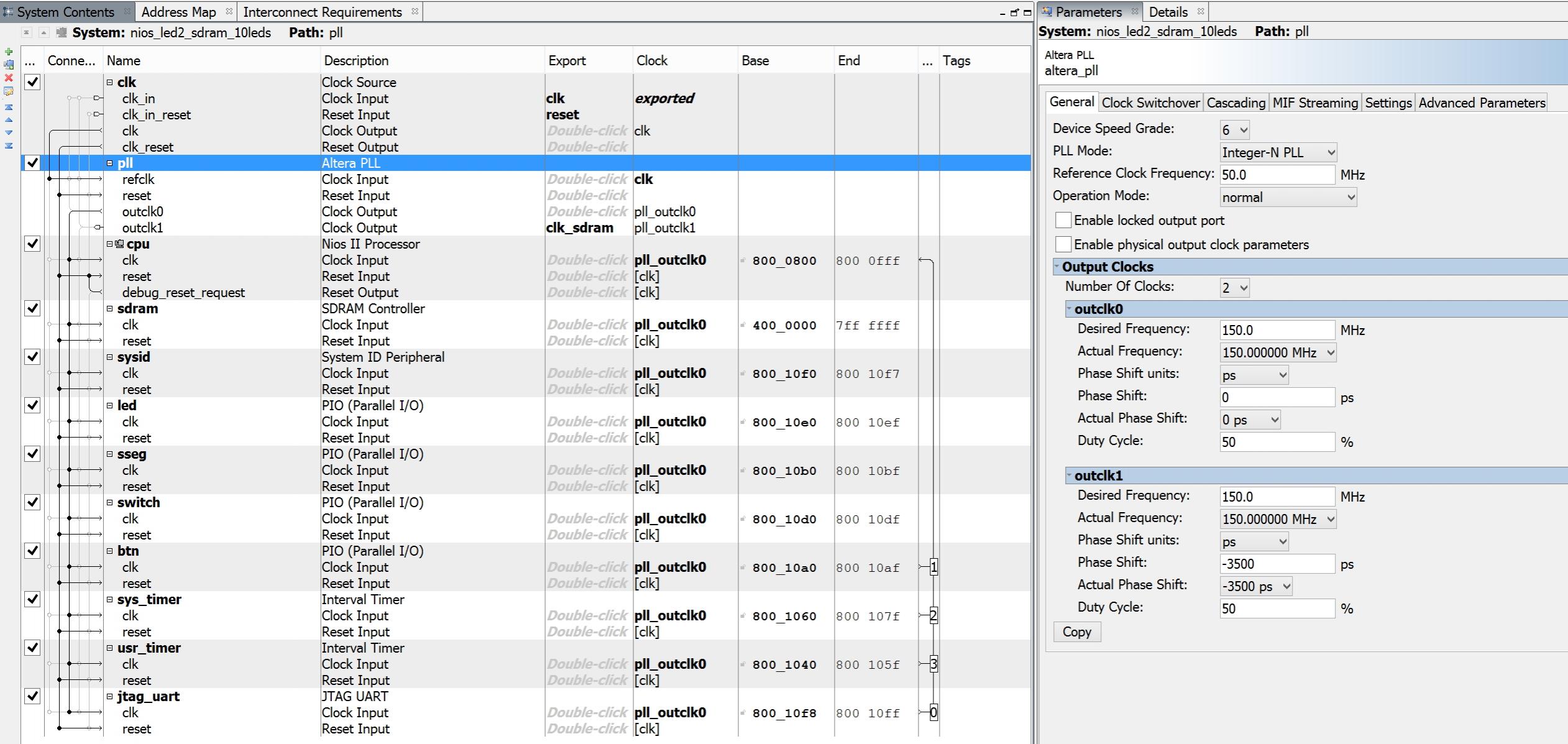
My case seems to be quite simple ... instantiation of one Qsys module. The Qsys module consists of (please have a look at Qsys screenshot below):- CPU
- PLL, that generates 2 clocks (1st – for all internal blocks, including CPU, 2nd – for external SDRAM)
- SDRAM controller, connected to external SDRAM
- GPIOs (buttons, switches, LEDs, 7-segment LEDs)
- 2 timers
module nios_led2_top (input clk,
	input  sw,
	input  key,
	output  led,
	output  hex3, hex2 , hex1, hex0,

	output  sdram_addr,
	inout  sdram_dq,
	output  sdram_bank,
	output sdram_cas_n, sdram_ras_n, sdram_cke, sdram_cs_n, sdram_clk,
	output sdram_dqmh, sdram_dqml, sdram_we_n);

	wire  sseg;
	assign hex3 = sseg;
	assign hex2 = sseg;
	assign hex1 = sseg;
	assign hex0 = sseg;

   nios_led2_sdram_10leds u0 (
		  .btn_export       (key),
		  .clk_clk          (clk),
		  .led_export     (led),
		  .reset_reset_n    (1'b1),
		  .sdram_wire_addr  (sdram_addr),
		  .sdram_wire_ba    (sdram_bank),
		  .sdram_wire_cas_n (sdram_cas_n),
		  .sdram_wire_cke   (sdram_cke),
		  .sdram_wire_cs_n  (sdram_cs_n),
		  .sdram_wire_dq    (sdram_dq),
		  .sdram_wire_dqm   ({sdram_dqmh, sdram_dqml}),
		  .sdram_wire_ras_n (sdram_ras_n),
		  .sdram_wire_we_n  (sdram_we_n),
		  .sseg_export      (sseg),
		  .switch_export    (sw),
		  .clk_sdram_clk    (sdram_clk)
    );
endmodule
The frequency of two PLL-generated clocks is 3 times input frequency (which is 50MHz). One of the clocks (that which clocks external SDRAM) is shifted -3.5ns in regard to another. I'm not sure if it's the optimal solution … this configuration I've adopted from a reference design of my board. Here is the content of the .sdc file: create_clock -name clk -period 20
create_clock -name {altera_reserved_tck} -period 40 {altera_reserved_tck}
derive_pll_clocks
derive_clock_uncertainty
set_input_delay -clock altera_reserved_tck -clock_fall 3
set_input_delay -clock altera_reserved_tck -clock_fall 3
set_output_delay -clock altera_reserved_tck 3
create_generated_clock -name clk_ext_sdram -source .gpll~PLL_OUTPUT_COUNTER|divclk}]
set_false_path -to
# Constraint SDRAM DATA for input
set_input_delay -clock clk_ext_sdram -max 0 ]
set_input_delay -clock clk_ext_sdram -min 0 ]
# Constraint SDRAM DATA for output
set_output_delay -clock clk_ext_sdram -max 0 ]
set_output_delay -clock clk_ext_sdram -min 0 ]
# Constraint DRAM ADDRESS for output
set_output_delay -clock clk_ext_sdram -max 0 ]
set_output_delay -clock clk_ext_sdram -min 0 ]
# Constraint SDRAM Controlss for output
set_output_delay -clock clk_ext_sdram -max 0 sdram_dqm* sdram_cas_n sdram_ras_n sdram_cke sdram_cs_n sdram_we_n}]
set_output_delay -clock clk_ext_sdram -min 0 sdram_dqm* sdram_cas_n sdram_ras_n sdram_cke sdram_cs_n sdram_we_n}]
set_multicycle_path -setup -to }] 2
set_multicycle_path -hold -to }] 1
set_false_path -from
set_false_path -from
set_false_path -from * -to
set_false_path -from * -to
In this constraint file I derived PLL clocks and used one of them to constraint SDRAM data, address and control signals (e.g. cs_n, cke, etc.). Doubtless, the constraints I imposed are erroneous … as Timing Analysis reported a lot of violations. These violations I've tried to repair with help of multicycles (again, perhaps, it's not the best solution for such issues). Anyway these multicycles constraints were ignored. Is it possible, just looking at the constraint file (and taking into count the information from Qsys) do the first estimation what is wrong with constraints ? Perhaps, correcting some basic errors can avoid the majority of timing violations. And then (after repairing big blunders) pass to timing analysis using TimeQuest reports?
- Mark as New
- Bookmark
- Subscribe
- Mute
- Subscribe to RSS Feed
- Permalink
- Report Inappropriate Content
So the clock you're using for the input constraint is the clock you're sending out. I assume the clock goes out and data comes back in. So the -max and -min values would represent the max and min external roundtrip delay from clock going out to data coming back in. I would plug those values in, as they're going to be large and their variation will determine if this is possible. After that's done, you will probably have to change the phase-shift, and most likely will need a multicycle since the data will be coming back more than one clock cycle after it was sent. I am worried about min/max variatino being too large, but we'll see.
Does the SDRAM read data at full rate, e.g. every clock that goes out you expect new data to come back, or is it slower?- Mark as New
- Bookmark
- Subscribe
- Mute
- Subscribe to RSS Feed
- Permalink
- Report Inappropriate Content
--- Quote Start --- So the clock you're using for the input constraint is the clock you're sending out. --- Quote End --- For gpios I use false_path, as timing is non relevant for buttons, switches, LEDs. Input/output contraints I applied only for sdram interface Yes, I use clock that goes out for input constraints (sdram data) and also for output constraints (all sdram signals - data/address/controls). This clock is derived from pll and its frequency is 150 MHz (3 times input external frequency). It's also -3.5ns shifted. There is also another PLL-derived clock that clocks SDRAM controller. It's frequency is also 150MHz, but as opposed to the first one, it isn't shifted. The SDRAM controller is responsible for generating all SDRAM interface signals - data, address, control signals. As I've already mentioned previously I'm not sure that it's the optimal solution, I've just picked it from reference design. So, let's resume:
- clock, used for input/output constraints is 150MHz, and has shift -3.5ns
- input/output signals are formed in SDRAM controller that is clocked by the 150MHz 0-shifted clock
- Mark as New
- Bookmark
- Subscribe
- Mute
- Subscribe to RSS Feed
- Permalink
- Report Inappropriate Content
Though I can't see your design details but my feeling is that your problem has nothing to do with io paths but is rather internal immediately before/after io.
You can check io paths report in Timequest. Your io sdc constraints of zero all over are the best ever for any design as it gives full clock period room but certainly that doesn't mean they are right but are very relaxing and unlikely to fail. so in short I think you are looking to associate io sdc constraints with reported failures but I don't see any connection. You better identify what paths are failing.- Mark as New
- Bookmark
- Subscribe
- Mute
- Subscribe to RSS Feed
- Permalink
- Report Inappropriate Content
The basic design details (e.g. Qsys screenshot, top-level Qsys wrapping (i.e. Qsys instantiation in the top module), constraints) I've mentioned in yesterday message.
Perhaps you are interested in the properties of other Qsys components (e.g. CPU) ... because in my previous mail only PLL properties are displayed. Today, about 3 hours ago, I've posted new message with more details on my design and answers to Ryan questions. But actually this message is pending for approving ... I hope it comes in 2 ... 3 hours. --- Quote Start --- my feeling is that your problem has nothing to do with io paths but is rather internal immediately before/after io. --- Quote End --- You mean metastability issues ? I've just checked "io paths report": 16 violations on SDRAM data bus. In order to have more chances for this message to be posted immediately (i.e. avoid pending-approving), I don't attach TimeQuest screenshot. If my guess is correct (i.e. you mean metastability), how to apprehend from this TimeQuest report, that these violations are caused by metastability, but not by some other issues ? --- Quote Start --- You better identify what paths are failing. --- Quote End --- The 16 SDRAM data signals fail to pass TimeQuest analysis.- Mark as New
- Bookmark
- Subscribe
- Mute
- Subscribe to RSS Feed
- Permalink
- Report Inappropriate Content
your failure reported (as per your previous post) violations from sdram_dq to za_data. So where is this path?
- Mark as New
- Bookmark
- Subscribe
- Mute
- Subscribe to RSS Feed
- Permalink
- Report Inappropriate Content
The failed paths (if inputs to fpga) are clocked out by clk_ext_sdram according to sdc but are latched on divclk. This has resulted in a setup relationship of 3.5 instead of 6.667 and is the root cause of problem. Why not latch input with same clock as sdram clock
- Mark as New
- Bookmark
- Subscribe
- Mute
- Subscribe to RSS Feed
- Permalink
- Report Inappropriate Content
--- Quote Start --- The failed paths (if inputs to fpga) are clocked out by clk_ext_sdram according to sdc but are latched on divclk. This has resulted in a setup relationship of 3.5 instead of 6.667 and is the root cause of problem. Why not latch input with same clock as sdram clock --- Quote End --- You mean why external sdram memory chip isn't clocked with the same clock as internal sdram controller ? This clocking schema I've picked from a reference design that was in support board package. By the way there was no any constraints on SDRAM interface I/O in the .sdc file.
- Mark as New
- Bookmark
- Subscribe
- Mute
- Subscribe to RSS Feed
- Permalink
- Report Inappropriate Content
--- Quote Start --- You mean why external sdram memory chip isn't clocked with the same clock as internal sdram controller ? This clocking schema I've picked from a reference design that was in support board package. By the way there was no any constraints on SDRAM interface I/O in the .sdc file. --- Quote End --- You are sending a clock to sdram chip as you have done (isn't it the clk_ext_sdram as named in your sdc). That is ok I am referring to your sdc constrains of set_input_delay/set_output_delay for sdram_dq. You are telling Timequest that sdram_dq data is clocked out from sdram chip on clk_ext_sdram. That is ok But you are latching it on divclk: is it also 150MHz and then why have you changed its phase. Although this clock of clk_ext_sdram is opposte data input but that is a trivial issue for now...
- Mark as New
- Bookmark
- Subscribe
- Mute
- Subscribe to RSS Feed
- Permalink
- Report Inappropriate Content
--- Quote Start --- But you are latching it on divclk: is it also 150MHz and then why have you changed its phase. Although this clock of clk_ext_sdram is opposte data input but that is a trivial issue for now... --- Quote End --- Yes, data that comes into FPGA (SDRAM controller IP to be precise) is latched by u0|pll|altera_pll_i|general[0].gpll~PLL_OUTPUT_COUNTER|divclk (which is PLL-derived clock with 0 phase shift). And the data launch clock is PLL-derived clock with -3.5ns phase shift, so the launch clock is about half-period "advanced" with respect to latch clock and respectively the latch clocks is half-period delayed with respect to launch clock. Correct ? Probably this half-period shift is intended to account for board propagation delay ? Anyway, if I properly understood, you propose to remove phase shift in launch clock. Correct ?
- Mark as New
- Bookmark
- Subscribe
- Mute
- Subscribe to RSS Feed
- Permalink
- Report Inappropriate Content
From your sdc commands I assume your sdram IF is not DDR. Hence why reduce available clock period by half?
- Mark as New
- Bookmark
- Subscribe
- Mute
- Subscribe to RSS Feed
- Permalink
- Report Inappropriate Content
--- Quote Start --- From your sdc commands I assume your sdram IF is not DDR --- Quote End --- Sorry, I didn't understand, what is "sdram IF"
- Mark as New
- Bookmark
- Subscribe
- Mute
- Subscribe to RSS Feed
- Permalink
- Report Inappropriate Content
SDRAM interface
- Mark as New
- Bookmark
- Subscribe
- Mute
- Subscribe to RSS Feed
- Permalink
- Report Inappropriate Content
No, according to SDRAM datasheet, it's clocked on positive edge. So, you propose to remove phase shift on u0|pll|altera_pll_i|general[1].gpll~PLL_OUTPUT_COUNTER|divclk and consequently on clk_ext_sdram ?
- Subscribe to RSS Feed
- Mark Topic as New
- Mark Topic as Read
- Float this Topic for Current User
- Bookmark
- Subscribe
- Printer Friendly Page