- Mark as New
- Bookmark
- Subscribe
- Mute
- Subscribe to RSS Feed
- Permalink
- Report Inappropriate Content
Hi,
I'm having some trouble defining a timing constraint for the attached circuit. A startsignal enables the first TFF and this again enables the second TFF (clk divider). The counter disables after counting 40 SCLK pulses the first TFF. The logic in black blox is a rising edge detector of a startsignal. I've created a generated clock constraint for the second TFF with the divide_by 2 attribute. TimeQuest gives me the following warning: Warning: Node: control:control_adc1|conf2adc:conf2adc|inst14 was determined to be a clock but was found without an associated clock assignment. Is TimeQuest assuming the output of the register "inst14" is a clock? I'm not using the output of that register as a clock. How would a proper constraining would look like? Another Issue I'm having is when I use Signal Tap II in my design the timing constraints can not be met: From Node control:control_adc1|conf2adc:conf2adc|lpm_shiftreg0:inst9|lpm_shiftreg:lpm_shiftreg_component|dffs[39] To Node sld_signaltap:auto_signaltap_0|sld_signaltap_impl:sld_signaltap_body|acq_trigger_in_reg[16] Launch Clock conf2adc_sclk_adc1 Latch Clock logic_analyzer_int Data Arrival Time 6769.609 Data Required Time 6760.259 Slack -9.350 (VIOLATED) Signal Tap II samples with 25 MHz. But the circuit under test operates with 3,25 MHz. Can I ignore the violated path because Signal Tap II samples with much higher frequency and therefore detects every events on the sampling node? Thanks.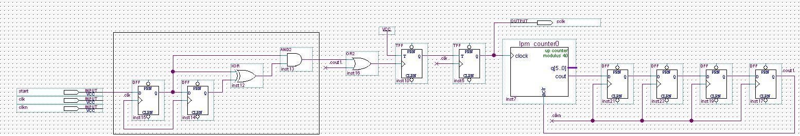
Link Copied
2 Replies
- Mark as New
- Bookmark
- Subscribe
- Mute
- Subscribe to RSS Feed
- Permalink
- Report Inappropriate Content
if you follow the clock input of inst10 back to the left you end up at the output of inst14
so inst14 "generates" the clock for inst10, well that is a gated clock ... should be avoided also inst5 is the clock source for inst7 this design is asyncronous, you better do a fully syncronous design where all FFs have the same clock source and you use clock enable functions of the FF instead of gates clocks. if you (or must) use more more than 1 clock source, use clock crossing circuits Have a look at the Quartus Handbook Chapter 6 : Recomended HDL Coding Styles well that is HDL design entry and not schematic design entry as you did, but there might be a documetation for this too.- Mark as New
- Bookmark
- Subscribe
- Mute
- Subscribe to RSS Feed
- Permalink
- Report Inappropriate Content
thanks for reply MSchmitt. I'll reconsider my design to make it synchronous.
Reply
Topic Options
- Subscribe to RSS Feed
- Mark Topic as New
- Mark Topic as Read
- Float this Topic for Current User
- Bookmark
- Subscribe
- Printer Friendly Page