- Mark as New
- Bookmark
- Subscribe
- Mute
- Subscribe to RSS Feed
- Permalink
- Report Inappropriate Content
Hi! In the qsys I have:
1. Clock Source 2. On-Chip Memory 3. Nios II Processor 4. System ID 5. JTAG UART 6. EPCS Serial Flash Controller 7. PIO 8. SDRAM Controller I want to use SDRAM (MT48LC4M32B2) to store instructions and data for NIOS application. In the NIOS II Processor properties reset vector is set to base address of EPCS controller. Exceptions vector is set to base address to SDRAM. In the NIOS EDS for Eclipce I can debug my application, it works. But in the NIOS flash programmer error occur: "Error: Error code: 4 for command: $SOPC_KIT_NIOS2/bin/nios2-flash-programmer "D:/Work/QuartusProjects/tests/test2/flash/test2_epcs_flash.flash" --base=0x2003800 --epcs --sidp=0x2004010 --id=0x0 --timestamp=1359654107 --device=1 --instance=0 '--cable=USB-Blaster on localhost [USB-0]' --program" What I did wrong? Thank youLink Copied
- Mark as New
- Bookmark
- Subscribe
- Mute
- Subscribe to RSS Feed
- Permalink
- Report Inappropriate Content
Flash Programmer works. But Processor not starts after power on. Anybody can help me? Thank you
- Mark as New
- Bookmark
- Subscribe
- Mute
- Subscribe to RSS Feed
- Permalink
- Report Inappropriate Content
Hi,
you have to store the fpga configuration data and the nios firmware in the EPCS. I'm using following script: sof2flash --input="fpga_design.sof" --output="fpga_design.flash" --epcs --verbose elf2flash --input="nios_firmware.elf" --output="pr4_top_fw.flash" --epcs --after="fpga_design.flash" --verbose nios2-flash-programmer --cable='USB-Blaster [USB-0]' --epcs --base=<EPCS Addr> fpga_design.flash nios2-flash-programmer --cable='USB-Blaster [USB-0]' --epcs --base=<EPCS Addr> nios_firmware.flash In my QSYS the reset vector is pointed to EPCS, the exception to onchip RAM because of faster ISRs. Verify in BSP Builder that all other sections are mapped to sdram. Then it should work. Jens- Mark as New
- Bookmark
- Subscribe
- Mute
- Subscribe to RSS Feed
- Permalink
- Report Inappropriate Content
Thank you for your reply! I have two EPCS devices, I use first to configure FPGA, and second to store NIOS program. Maybe it not start because SDRAM pins not enabled with the Fast Input Register and Fast Output Register logic options or PLL is tuned incorrectly? ("Symptoms of an Untuned PLL" p.2-11 in Embedded Peripherals IP User Guide)
- Mark as New
- Bookmark
- Subscribe
- Mute
- Subscribe to RSS Feed
- Permalink
- Report Inappropriate Content
If you can debug the firmware whitin the sdram it should work correct. Before debugging the debugger performs a verify of your code stored in the sdram.
The EPCS Controller executes after startup a small piece of code the boot loader. (file your_sopc_epcs_controller_boot_rom_synth.hex in the sopc subdirectories) How does the boot loader know from which EPCS the code should be loaded? Jens- Mark as New
- Bookmark
- Subscribe
- Mute
- Subscribe to RSS Feed
- Permalink
- Report Inappropriate Content
Since the FGPA hardware doesn't access your second EPCS16 chip, you could actually write the nios code image to it in any format you like!
You can then write some boot code to copy it to SDRAM and put that into an internal memory block that is initialised when the fpga image is loaded (and is pointed to by the nios's reset vector). Since you can link the boot code to the correct address it should be easy to write!- Mark as New
- Bookmark
- Subscribe
- Mute
- Subscribe to RSS Feed
- Permalink
- Report Inappropriate Content
*.hex file exist in "synthesis" folder. The first EPCS connected to a FPGA configuration pins. The second EPCS device connected to the regular I/O pins, EPCS flash Controller in Qsys assigned to this pins. Reset vector is set to this EPCS Controller. Is this configuration correct?
- Mark as New
- Bookmark
- Subscribe
- Mute
- Subscribe to RSS Feed
- Permalink
- Report Inappropriate Content
Thank you, dsl! But I don't know, how to write a boot code...Where I can read about this?
- Mark as New
- Bookmark
- Subscribe
- Mute
- Subscribe to RSS Feed
- Permalink
- Report Inappropriate Content
It should be an option to use the quartus generated boot code if you use just the second EPCS with the controller. Does the configuration of fpga from the other EPCS work fine?
- Mark as New
- Bookmark
- Subscribe
- Mute
- Subscribe to RSS Feed
- Permalink
- Report Inappropriate Content
another idea for starting: try at first to put all *.flash (as i described above) in the first EPCS and assign the EPCS controller in qsys to that EPCS. Ignore for bring up your hardware the second EPCS. After you know that this part of your hardware works correct you can start bring up the rest.
- Mark as New
- Bookmark
- Subscribe
- Mute
- Subscribe to RSS Feed
- Permalink
- Report Inappropriate Content
Thank you! I'll try to do this. My computer is very slow, it will take a lot of time to compile the project....I'll answer late
- Mark as New
- Bookmark
- Subscribe
- Mute
- Subscribe to RSS Feed
- Permalink
- Report Inappropriate Content
Thank you! A am already doing that)) I'll answer later, my computer is very slow, it take a lot of time to recompile the project
- Mark as New
- Bookmark
- Subscribe
- Mute
- Subscribe to RSS Feed
- Permalink
- Report Inappropriate Content
Boot code is just code that copies data from the boot device (in this case the EPCS device) and main memory.
An ELF program (as output by ld) has 'program headers' (run objdump -p) that make it very simple to load. To get C code running on the nios you need asm instructions to set %sp and %gp and then jump to the C function (don't call it main()). I've never had to access EPCS type memory - but it can't be hard!- Mark as New
- Bookmark
- Subscribe
- Mute
- Subscribe to RSS Feed
- Permalink
- Report Inappropriate Content
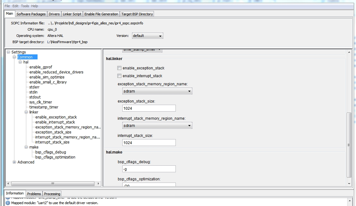
If in the Linker Script tab of the BSP Editor I set all of Linker Region Name to on-chip memory my system works and boot from EPCS after power on. If I set all of Linker Region Name to SDRAM it not works, but I can launche it and debug...I don't understand why
- Mark as New
- Bookmark
- Subscribe
- Mute
- Subscribe to RSS Feed
- Permalink
- Report Inappropriate Content
Did you recompile and reflash the EPCS after changing the linker sections?
- Mark as New
- Bookmark
- Subscribe
- Mute
- Subscribe to RSS Feed
- Permalink
- Report Inappropriate Content
Yes, I did
- Mark as New
- Bookmark
- Subscribe
- Mute
- Subscribe to RSS Feed
- Permalink
- Report Inappropriate Content
- Mark as New
- Bookmark
- Subscribe
- Mute
- Subscribe to RSS Feed
- Permalink
- Report Inappropriate Content
- Mark as New
- Bookmark
- Subscribe
- Mute
- Subscribe to RSS Feed
- Permalink
- Report Inappropriate Content
- Mark as New
- Bookmark
- Subscribe
- Mute
- Subscribe to RSS Feed
- Permalink
- Report Inappropriate Content
I mapped all sections to on-chip memory, rebuild project and from Flash Programmer write *.elf to EPCS. After that my system boot from EPCS, I can see it from Signal Tap Logic Analyzer. There is a PIO-out, which say me, that NIOS is working (and signals of two sgdma). When I mapped all of sections to SDRAM, this signal is always zero (and signals of sgdma too).
- Mark as New
- Bookmark
- Subscribe
- Mute
- Subscribe to RSS Feed
- Permalink
- Report Inappropriate Content
Have you tried writing code that does a memory test of the SDRAM?
- Subscribe to RSS Feed
- Mark Topic as New
- Mark Topic as Read
- Float this Topic for Current User
- Bookmark
- Subscribe
- Printer Friendly Page