- Mark as New
- Bookmark
- Subscribe
- Mute
- Subscribe to RSS Feed
- Permalink
- Report Inappropriate Content
Dear Sir,
I'm trying to configure the Cyclone V transceiver in order to establish a SATA I connection.
Unfortunately, I don't know if my actual configuration is the right one.
The problem is the initial OOB sequence. The OOB sequence expects these steps: 1) the Host (FPGA) sends a COMRESET primitive; 2) the device (HDD) sends a COMINIT primitive; 3) the Host sends a COMWAKE primitive; 4) the device sends a COMWAKE primitive.
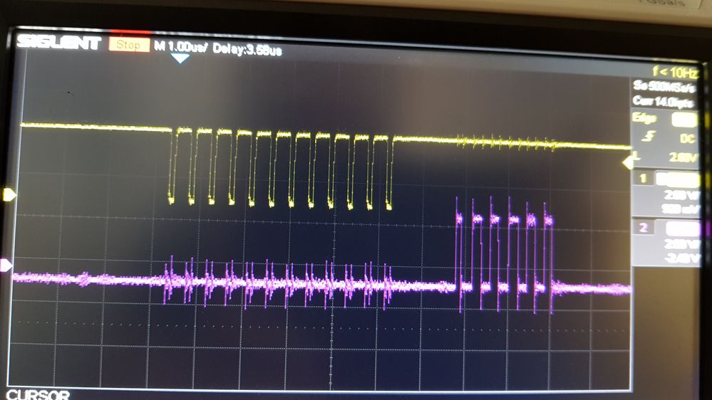
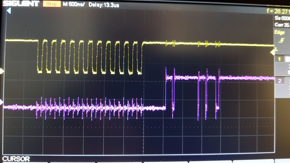
You can see what happens in the attached figure.
In the two figures, in yellow you can see the XCVR TX electric idle, in pink you can see the XCVR TX signal detect.
In the first figure, the host sends the COMRESET and the device sends the COMINIT.
In the second figure, the host sends the COMWAKE, but it does not receive the COMWAKE response.
I think that this can happen because there is some problem with the XCVR configuration.
The cyclone V that I'm using is: 5CGXFC3B6F23I7 and I'm using the XCVR with the external fPLL
The XCRV assignment that I'm using are:
cfast_sata_rx_p Location PIN_W2
cfast_sata_tx_p Location PIN_U2
cfast_sata_rx_p Receiver Signal Detection Unit Enable/Disable On
cfast_sata_rx_p Receiver Signal Detection Voltage Threshold 7
cfast_sata_rx_p Receiver Cycle Count Before Signal Detect Block Declares Loss Of Signal 1
cfast_sata_rx_p Receiver Cycle Count Before Signal Detect Block Declares Presence Of Signal 2
cfast_sata_tx_p Transmitter Slew Rate Control 3
cfast_sata_tx_p Transceiver Analog Settings Protocol SATA1_M
cfast_sata_rx_p Transceiver Analog Settings Protocol SATA1_M
Are these assignments the right one?
Please, can you take a look at the XCVR, PHY reset controller, XCVR reconfiguration IP files and at the project files?
Link Copied
- Mark as New
- Bookmark
- Subscribe
- Mute
- Subscribe to RSS Feed
- Permalink
- Report Inappropriate Content
Hi,
As I understand it, you are running SATA Gen1m with CV XCVR and observe some issue with the RX signal detect during the OOB init sequence. If I understand it correctly, you have configured the signal detect settings following the Altera XCVR PHY IP Core user guide -> "Enable rx_std_signaldetect port" section for Cyclone V Transceiver Native PHY IP Core.
The following are the assignments from user guide:
• set_instance_assignment -name XCVR_RX_SD_ENABLE ON
• set_instance_assignment -name XCVR_RX_SD_THRESHOLD 7
• set_instance_assignment -name XCVR_RX_COMMON_MODE_VOLTAGE VTT_OP55V
• set_instance_assignment -name XCVR_RX_SD_OFF 1
• set_instance_assignment -name XCVR_RX_SD_ON 2
Mind cross check with your QSF assignments to see if there is any discrepancy?
If the assignment is the same with user guide already, you can try with the following set of settings to see if it helps:
• set_instance_assignment -name XCVR_RX_SD_ENABLE ON
• set_instance_assignment -name XCVR_RX_SD_THRESHOLD 5
• set_instance_assignment -name XCVR_RX_COMMON_MODE_VOLTAGE VTT_OP65V
• set_instance_assignment -name XCVR_RX_SD_OFF 3
• set_instance_assignment -name XCVR_RX_SD_ON 5
Please let me know if there is any concern. Thank you.
Best regards,
Chee Pin
- Mark as New
- Bookmark
- Subscribe
- Mute
- Subscribe to RSS Feed
- Permalink
- Report Inappropriate Content
Dear Sir,
I made several tries and I found a configuration that allows detecting the COMWAKE signal.
The configuration that works for me is:
cfast_sata_rx_p Receiver Signal Detection Unit Enable/Disable On
cfast_sata_rx_p Receiver Signal Detection Voltage Threshold 7
cfast_sata_rx_p Receiver Cycle Count Before Signal Detect Block Declares Loss Of Signal 0
cfast_sata_rx_p Receiver Cycle Count Before Signal Detect Block Declares Presence Of Signal 2
cfast_sata_tx_p Transceiver Analog Settings Protocol SATA1_M
cfast_sata_rx_p Transceiver Analog Settings Protocol SATA1_M
Now I have another problem with the signal detect.
After the COMWAKE signal, the SATA protocol requires that the FPGA receives 54.6us of ALIGN primitive at 6 Gbps, 54.6us of ALIGN primitive at 3 Gbps and 54.6us of ALIGN primitive at 1.5 Gbps.
My signal detect behavior is like this:
I have a stable signal detect for the first 109.2us (54.6us of ALIGN primitive at 6 Gbps and 54.6us of ALIGN primitive at 3 Gbps), but a not stable signal detect for the last 54.6us.
The questions are:
1) Does the SIGNAL DETECT not stable means that the Native PHY is not working properly?
2) Is the SIGNAL DETECT not stable because I set the "Receiver Cycle Count Before Signal Detect Block Declares Loss Of Signal" to 0?
- Mark as New
- Bookmark
- Subscribe
- Mute
- Subscribe to RSS Feed
- Permalink
- Report Inappropriate Content
Hi,
Sorry for the delay. Regarding your latest inquiries, please see my responses as following:
Q1 - Generally signal detect would be dependent on the settings that you configure in QSF assignment and the signal quality that go into the receiver.
Q2 - It is rather difficult to tell what might be causing the signal detect signal not stable based on the current observation. Probably you can try to play around with the specific assignment that you suspected by setting to other values to see if it helps.
Thank you.
Best regards,
Chee Pin
- Mark as New
- Bookmark
- Subscribe
- Mute
- Subscribe to RSS Feed
- Permalink
- Report Inappropriate Content
Hi,
Unfortunately, I can't change the QSF assignment, because if I change it, my OOB sequence does not finish.
Now the question is: Should I assume that in each cycle in which the signal detect is low the PHY output data are corrupted?
Thank you.
- Mark as New
- Bookmark
- Subscribe
- Mute
- Subscribe to RSS Feed
- Permalink
- Report Inappropriate Content
Hi,
For your information signal detect behavior would be dependent on the threshold settings. Even when this signal is low, we cannot conclude that the PHY output data is corrupted. To tell if the RX is working fine, generally we would first look at the CDR status signals to see if it still lock-to-data or already lose lock-to-data. If the CDR is still in lock-to-data mode, if there is any bit error observed, then we would need to check the signal integrity of the signal at the RX input pin.
Thank you.
- Subscribe to RSS Feed
- Mark Topic as New
- Mark Topic as Read
- Float this Topic for Current User
- Bookmark
- Subscribe
- Printer Friendly Page


