- Mark as New
- Bookmark
- Subscribe
- Mute
- Subscribe to RSS Feed
- Permalink
- Report Inappropriate Content
Hi,
I can't seem to find this information anywhere. I need to design a PCB that has a DDR3 memory socket and and FPGA that would interact with the RAM memory plugged into the socket. Now my problem is: the memory controller offered in Quartus expects the memory timings to be put in before I generate the IP. I know that the memory timings can be read from the EEPROM doing an SPD test. Is it possible to dynamically reconfigure the Memory Controller IP, and is it possible at all to interface with RAM sticks with different memory timings?
Thanks
Link Copied
- Mark as New
- Bookmark
- Subscribe
- Mute
- Subscribe to RSS Feed
- Permalink
- Report Inappropriate Content
Hi Gabe,
I'm Adzim. Thanks for using the Intel Community.
May I know which device that you're used?
Based on your question, do you want to create your own custom memory controller?
"is it possible at all to interface with RAM sticks with different memory timings"
I'm not clear about this. Where is the memory timings here refer to?
Regards,
Adzim
- Mark as New
- Bookmark
- Subscribe
- Mute
- Subscribe to RSS Feed
- Permalink
- Report Inappropriate Content
Hi Adzim,
Sorry for being ambiguous.
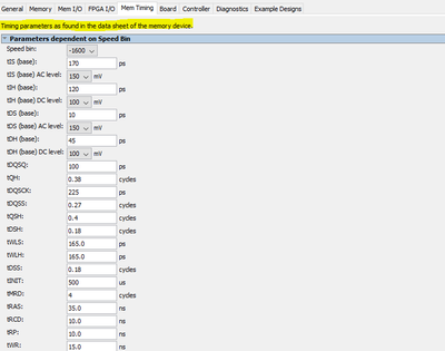
I am planning to use the Quartus Arria 10 EMIF IP. When I configure the EMIF IP in Qsys, I have to specify the memory timings:
The problem is: these values are specific to a memory chip. However, I would like to be able to use a range of DDR3 DIMM memory sticks (that might have different memory chips on it, therefore different memory timings) with this EMIF IP. The question is: Does the DDR3 controller provided in Quartus re-adjust the memory timings dynamically, or would I have to regenerate the IP for each memory stick that I plan to use?
Let me know if this clarified things a bit
- Mark as New
- Bookmark
- Subscribe
- Mute
- Subscribe to RSS Feed
- Permalink
- Report Inappropriate Content
Hi Gabe,
Thanks for clarifying your intentions.
Basically every memory timing must be configured according to the datasheet of the memory device.
Then the IP can be generated for the device.
If everything is configured correctly, the memory device should be working.
If the device is using the different memory timings, your design might encounter some errors such as timing violations or calibration error.
So I think generating each IP for your memory devices should be the best way to simulate your project.
I don't think that re-adjust the memory timings internally is a good way because you might be setting the value wrongly.
Regards,
Adzim
- Mark as New
- Bookmark
- Subscribe
- Mute
- Subscribe to RSS Feed
- Permalink
- Report Inappropriate Content
Hi Gabe,
Do you still got question on this topic?
Regards,
Adzim
- Subscribe to RSS Feed
- Mark Topic as New
- Mark Topic as Read
- Float this Topic for Current User
- Bookmark
- Subscribe
- Printer Friendly Page
