- Mark as New
- Bookmark
- Subscribe
- Mute
- Subscribe to RSS Feed
- Permalink
- Report Inappropriate Content
Hello,
I am designing a custom board with Cyclone 10 LP FPGA - 10CL080YU484A7G. I have the following questions:
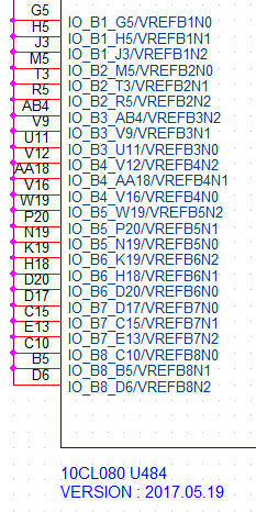
a) Should the VREFB pins be connected to Ground or VCCIO? I use same IO voltage of 1.2V for all banks.
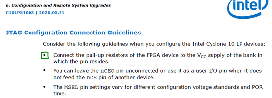
b) Cyclone 10 Handbook mentions that pull up resistors of FPGA device to be connected to VCC of the bank in which the JTAG pins reside. I do not understand this point. Could you please elaborate? Is this a setting in Quartus Prime? Or any connections to be made in the board schematics?
Is this anything related to RUP and RDN pins of FPGA? I am using some of the RUP and RDN as user IO.
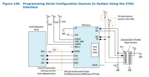
I am using the SFL core for in system configuration using JTAG. Supply voltage to JTAG connector is VCCA (2.5 V in my case). If JTAG signals are at VCCA (2.5V logic) and VCCIO of FPGA is 3.3V, will this work?
Thank you!
Link Copied
- Mark as New
- Bookmark
- Subscribe
- Mute
- Subscribe to RSS Feed
- Permalink
- Report Inappropriate Content
Hello,
Please refer to these links for your reference design:
1. Cyclone 10 LP GPIO User Guide: https://www.intel.com/content/dam/www/programmable/us/en/pdfs/literature/hb/cyclone-10/c10lp-51003.pdf
2. Cyclone 10 LP Device Datasheet: https://www.intel.com/content/dam/www/programmable/us/en/pdfs/literature/hb/cyclone-10/c10lp-51002.pdf
3. Cyclone 10 LP Pin Connection Guideline: https://www.intel.com/content/dam/www/programmable/us/en/pdfs/literature/dp/cyclone-10/pcg-01021.pdf
The answer is yes to the second question. You can use Pin Planner to program this setting.
Please refer to I/O Standard table from page 78 and see your setting meet the guideline.
Thank you.
- Mark as New
- Bookmark
- Subscribe
- Mute
- Subscribe to RSS Feed
- Permalink
- Report Inappropriate Content
Hello,
Thank you for your answer. I have referred the documents.
It is still not clear for me: "pull up resistors of FPGA device to be connected to VCC of the bank in which the JTAG pins reside"
The above diagram shows the JTAG connector pins are connected to VCCA, which is 2.5 V and FPGA pull ups connected to VCC of the bank i.e VCCIO = 3.3V. Is this not a mismatch?
- Mark as New
- Bookmark
- Subscribe
- Mute
- Subscribe to RSS Feed
- Permalink
- Report Inappropriate Content
Hello,
That is the guideline where you configure Intel Cyclone 10 LP Device where you need to connect the pull up resistor of the device to Vcc in which the pin resides.
You can configure pins using Pin Planner.
- Subscribe to RSS Feed
- Mark Topic as New
- Mark Topic as Read
- Float this Topic for Current User
- Bookmark
- Subscribe
- Printer Friendly Page


