- Mark as New
- Bookmark
- Subscribe
- Mute
- Subscribe to RSS Feed
- Permalink
- Report Inappropriate Content
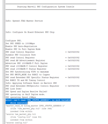
I am attempting to use the aforementioned design which can be found here with the Arria V GX 5AGXFB3H4F35C4N. This code was meant for a different Arria V GX, but I switched it to the proper board. I am currently trying to implement some of the tests mentioned at the bottom of the document, but running the source.tcl script leaves me with the following errors:
If anyone has suggestions on how to begin setting up this design properly it would be appreciated. It would also be helpful if anyone had insights as to how to send data from the board to my pc through the ethernet cable.
Link Copied
- Mark as New
- Bookmark
- Subscribe
- Mute
- Subscribe to RSS Feed
- Permalink
- Report Inappropriate Content
Hi,
Let's clarify few things here.
- The reference design consists of traffic generator/checker + TSE MAC + external PHY chip where user can choose perform internal loopback testing or external loopback on board. Intel Ethernet IP solution only cover till Ethernet data link layer where the MAC resides. Anything above data link layer protocol needs to be implemented by user own application design
- I presume you are porting over the reference design to your own board. Have you cross check the design difference other than just a change in Arria V FPGA ? How about your overall hardware system connection like using same external PHY chip and it's setting ? FPGA reset and clocking management ? The design difference is likely the answer why the TCL script run is failing
One of the debug recommendation is always start with TSE internal loopback test first. This will help to isolate whether the failure resides inside FPGA or outside at the board level
Thanks.
Regards,
dlim
- Mark as New
- Bookmark
- Subscribe
- Mute
- Subscribe to RSS Feed
- Permalink
- Report Inappropriate Content
I attempted to find a reference manual for the board the code was meant for which is the Arria V GX 5AGXFB3H6F35C6ES, but could not find anything specific to this board. I am not sure if I am looking into the wrong places or not. As far as I know, both boards are using the same PHY chip, and I have checked the pin outputs for the qsf file and it all seems to match up except for the DEVICE_FILTER_SPEED_GRADE where the original board was 6_H6 and my board (Arria V GX 5AGXFB3H4F35C4N) is only 5_H5. Outside of matching the pins up and switching the board in device assignment, I currently have not made any changes to the config settings. Is there anywhere I could find a reference manual for the original board so I could compare the two?
- Mark as New
- Bookmark
- Subscribe
- Mute
- Subscribe to RSS Feed
- Permalink
- Report Inappropriate Content
HI,
Sorry for the late reply, based on AN647 doc, the reference design should be developed for following Arria V GX dev kit. You can download the dev kit user guide from below link as well
Thanks.
Regards,
dlim
- Mark as New
- Bookmark
- Subscribe
- Mute
- Subscribe to RSS Feed
- Permalink
- Report Inappropriate Content
HI,
I hope I have addressed your enquiry on ref design usage based on my feedback in Aug 17.
For now, I am setting this case to closure.
Thanks.
Regards,
dlim
- Subscribe to RSS Feed
- Mark Topic as New
- Mark Topic as Read
- Float this Topic for Current User
- Bookmark
- Subscribe
- Printer Friendly Page
