- Als neu kennzeichnen
- Lesezeichen
- Abonnieren
- Stummschalten
- RSS-Feed abonnieren
- Kennzeichnen
- Anstößigen Inhalt melden
Hi guys i am doing synthesis at module level and IO buffers are being implemented by the tool..
I dont want these buffers to be implemented. Can anybody help me with the constraints for not inferring a buffer at input and output portsLink kopiert
- Als neu kennzeichnen
- Lesezeichen
- Abonnieren
- Stummschalten
- RSS-Feed abonnieren
- Kennzeichnen
- Anstößigen Inhalt melden
Add the assignment Virtual Pin to the pins you don't want to go to I/O. I recommend minimally not doing this to the clock though, otherwise it gets placed internally and uses local routing to get to a global.
- Als neu kennzeichnen
- Lesezeichen
- Abonnieren
- Stummschalten
- RSS-Feed abonnieren
- Kennzeichnen
- Anstößigen Inhalt melden
- Als neu kennzeichnen
- Lesezeichen
- Abonnieren
- Stummschalten
- RSS-Feed abonnieren
- Kennzeichnen
- Anstößigen Inhalt melden
Yes.
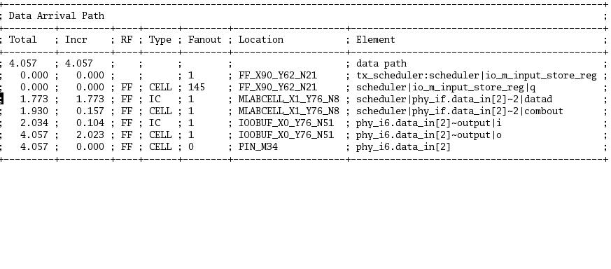
The 2ns IO buffer delay will go away. I also wonder if that long IC delay will go away too. If that FF feeds a lot of I/O that are placed around the die, it will have terrible timing. That being said, you currently have a timing constraint on the I/O for it to be analyzed. I find it difficult to analyze I/O on a sub-module that won't be I/O once it's all hooked together. Your timing depends so much on what it drives and where it's placed, it's really hard to do correctly. I tend to leave that for integration(but try to make sure the connections are as short as possible, i.e. register the outputs)- Als neu kennzeichnen
- Lesezeichen
- Abonnieren
- Stummschalten
- RSS-Feed abonnieren
- Kennzeichnen
- Anstößigen Inhalt melden
Yes the flip flop does feed too many mux and mux only and then the mux out is being drived to the output and yes i am facing timing issues to a bigger extent.
Actually the code wasnt written by me i have to do the synthesis only. Just tell me one thing can a path such as Flop->mux->output a desirable logic. i doubt that since a combo logic is feeding the outputs it maybe a reason for larger delays. And ya the clock to the module i am constraining is 225Mhz. It will be helpful for me if u can comment on this. :)- Als neu kennzeichnen
- Lesezeichen
- Abonnieren
- Stummschalten
- RSS-Feed abonnieren
- Kennzeichnen
- Anstößigen Inhalt melden
I'm not following. I assumed this block really fed something else internally(another hierarchy). But it sounds like it's real? For 225MHz you almost have to push the register into the I/O cell, which means there will be no logic between the output reg and the IO.
- Als neu kennzeichnen
- Lesezeichen
- Abonnieren
- Stummschalten
- RSS-Feed abonnieren
- Kennzeichnen
- Anstößigen Inhalt melden
Ok I get you.
I will try duplicating the registers in order to reduce the fanout. And thanks for your suggestion you reduced my work a lot. :)- RSS-Feed abonnieren
- Thema als neu kennzeichnen
- Thema als gelesen kennzeichnen
- Diesen Thema für aktuellen Benutzer floaten
- Lesezeichen
- Abonnieren
- Drucker-Anzeigeseite