- Mark as New
- Bookmark
- Subscribe
- Mute
- Subscribe to RSS Feed
- Permalink
- Report Inappropriate Content
I created Flash Update module with Qsys
    onchip_flash_0 : component altera_onchip_flash
        generic map (
            INIT_FILENAME                       => "",
            INIT_FILENAME_SIM                   => "",
            DEVICE_FAMILY                       => "MAX 10",
            PART_NAME                           => "10M50DAF484C7G",
            DEVICE_ID                           => "50",
            SECTOR1_START_ADDR                  => 0,
            SECTOR1_END_ADDR                    => 8191,
            SECTOR2_START_ADDR                  => 8192,
            SECTOR2_END_ADDR                    => 16383,
            SECTOR3_START_ADDR                  => 16384,
            SECTOR3_END_ADDR                    => 114687,
            SECTOR4_START_ADDR                  => 114688,
            SECTOR4_END_ADDR                    => 188415,
            SECTOR5_START_ADDR                  => 188416,
            SECTOR5_END_ADDR                    => 360447,
            MIN_VALID_ADDR                      => 0,
            MAX_VALID_ADDR                      => 360447,
            MIN_UFM_VALID_ADDR                  => 0,
            MAX_UFM_VALID_ADDR                  => 16383,
            SECTOR1_MAP                         => 1,
            SECTOR2_MAP                         => 2,
            SECTOR3_MAP                         => 3,
            SECTOR4_MAP                         => 4,
            SECTOR5_MAP                         => 5,
            ADDR_RANGE1_END_ADDR                => 360447,
            ADDR_RANGE1_OFFSET                  => 2048,
            ADDR_RANGE2_OFFSET                  => 0,
            AVMM_DATA_ADDR_WIDTH                => 19,
            AVMM_DATA_DATA_WIDTH                => 32,
            AVMM_DATA_BURSTCOUNT_WIDTH          => 4,
            SECTOR_READ_PROTECTION_MODE         => 0,
            FLASH_SEQ_READ_DATA_COUNT           => 4,
            FLASH_ADDR_ALIGNMENT_BITS           => 2,
            FLASH_READ_CYCLE_MAX_INDEX          => 5,
            FLASH_RESET_CYCLE_MAX_INDEX         => 7,
            FLASH_BUSY_TIMEOUT_CYCLE_MAX_INDEX  => 36,
            FLASH_ERASE_TIMEOUT_CYCLE_MAX_INDEX => 10500000,
            FLASH_WRITE_TIMEOUT_CYCLE_MAX_INDEX => 9150,
            PARALLEL_MODE                       => true,
            READ_AND_WRITE_MODE                 => true,
            WRAPPING_BURST_MODE                 => false,
            IS_DUAL_BOOT                        => "False",
            IS_ERAM_SKIP                        => "True",
            IS_COMPRESSED_IMAGE                 => "True"
        )
        port map (
            clock                   => clock,                   --    clk.clk
            reset_n                 => reset_n,                 -- nreset.reset_n
            avmm_data_addr          => avmm_data_addr,          --   data.address
            avmm_data_read          => avmm_data_read,          --       .read
            avmm_data_writedata     => avmm_data_writedata,     --       .writedata
            avmm_data_write         => avmm_data_write,         --       .write
            avmm_data_readdata      => avmm_data_readdata,      --       .readdata
            avmm_data_waitrequest   => avmm_data_waitrequest,   --       .waitrequest
            avmm_data_readdatavalid => avmm_data_readdatavalid, --       .readdatavalid
            avmm_data_burstcount    => avmm_data_burstcount,    --       .burstcount
            avmm_csr_addr           => avmm_csr_addr,           --    csr.address
            avmm_csr_read           => avmm_csr_read,           --       .read
            avmm_csr_writedata      => avmm_csr_writedata,      --       .writedata
            avmm_csr_write          => avmm_csr_write,          --       .write
            avmm_csr_readdata       => avmm_csr_readdata        --       .readdata
        );
In oreder to have two images - bootloader(CFM0) and main program(CFM1-CFM2) - I need Dual Compressed Images. So I set - Assignments -> Device -> Devise and Pin Options -> Configuration -> Dual Compressed Images And generics in Flash Update module I set
IS_DUAL_BOOT        => "True",
IS_ERAM_SKIP        => "True",
IS_COMPRESSED_IMAGE => "True"
When I compile I get an error --- Quote Start --- Error (169130): Configuration mode specified as Remote but remote update block is not found in design --- Quote End --- If I set Assignments -> Device -> Devise and Pin Options -> Configuration -> Single Compressed Image And generics
IS_DUAL_BOOT        => "False",
IS_ERAM_SKIP        => "True",
IS_COMPRESSED_IMAGE => "True"
It compiles without error. If I set Assignments -> Device -> Devise and Pin Options -> Configuration -> Single Compressed Image And generics
IS_DUAL_BOOT        => "True",
IS_ERAM_SKIP        => "True",
IS_COMPRESSED_IMAGE => "True"
I get an error --- Quote Start --- Error (14740): Configuration mode on atom "bootloader:U_BOOTLOADER|flash_update:U_FLASH_UPDATE|altera_onchip_flash : nchip_flash_0|altera_onchip_flash_block:altera_onchip_flash_block|ufm_block" does not match the project setting. Update and regenerate the Qsys system to match the project setting. --- Quote End --- How can I compile for Dual Compressed Images?
Link Copied
- Mark as New
- Bookmark
- Subscribe
- Mute
- Subscribe to RSS Feed
- Permalink
- Report Inappropriate Content
Hi,
Have you set the correct parameter setting of Nios ll and on-chip ram? Delete the incremental_db and db folder and recheck. Refer the document for steps. http://caxapa.ru/thumbs/592124/an730.pdf Let me know if this has helped resolve the issue you are facing or if you need any further assistance. Best Regards, Anand Raj Shankar (This message was posted on behalf of Intel Corporation)- Mark as New
- Bookmark
- Subscribe
- Mute
- Subscribe to RSS Feed
- Permalink
- Report Inappropriate Content
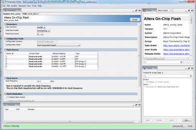
--- Quote Start --- Hi, Have you set the correct parameter setting of Nios ll and on-chip ram? Delete the incremental_db and db folder and recheck. Refer the document for steps. http://caxapa.ru/thumbs/592124/an730.pdf Let me know if this has helped resolve the issue you are facing or if you need any further assistance. Best Regards, Anand Raj Shankar (This message was posted on behalf of Intel Corporation) --- Quote End --- I don't have NiosII in my project. It's QSYS generated core. I go Tools->IP Catalog->Library->Basic Functions->On Chip Memory->Altera On-Chip Flash.https://alteraforum.com/forum/attachment.php?attachmentid=15108&stc=1 I deleted the incremental_db and db folder - it didn't help.
- Mark as New
- Bookmark
- Subscribe
- Mute
- Subscribe to RSS Feed
- Permalink
- Report Inappropriate Content
As it says, you need to have the RSU block in your design to use dual compressed images. See these online trainings:
https://www.altera.com/support/training/course/omaxrsu101.html https://www.altera.com/support/training/course/omaxrsu102.html- Mark as New
- Bookmark
- Subscribe
- Mute
- Subscribe to RSS Feed
- Permalink
- Report Inappropriate Content
--- Quote Start --- As it says, you need to have the RSU block in your design to use dual compressed images. See these online trainings: https://www.altera.com/support/training/course/omaxrsu101.html https://www.altera.com/support/training/course/omaxrsu102.html --- Quote End --- I see. Thank you. Well...I created Altera On-Chip Flash module and Altera Dual Configuration module.
component flash_update is
    port (
        clock                   : in  std_logic                     := '0';             --    clk.clk
        avmm_csr_addr           : in  std_logic                     := '0';             --    csr.address
        avmm_csr_read           : in  std_logic                     := '0';             --       .read
        avmm_csr_writedata      : in  std_logic_vector(31 downto 0) := (others => '0'); --       .writedata
        avmm_csr_write          : in  std_logic                     := '0';             --       .write
        avmm_csr_readdata       : out std_logic_vector(31 downto 0);                    --       .readdata
        avmm_data_addr          : in  std_logic_vector(18 downto 0) := (others => '0'); --   data.address
        avmm_data_read          : in  std_logic                     := '0';             --       .read
        avmm_data_writedata     : in  std_logic_vector(31 downto 0) := (others => '0'); --       .writedata
        avmm_data_write         : in  std_logic                     := '0';             --       .write
        avmm_data_readdata      : out std_logic_vector(31 downto 0);                    --       .readdata
        avmm_data_waitrequest   : out std_logic;                                        --       .waitrequest
        avmm_data_readdatavalid : out std_logic;                                        --       .readdatavalid
        avmm_data_burstcount    : in  std_logic_vector(3 downto 0)  := (others => '0'); --       .burstcount
        reset_n                 : in  std_logic                     := '0'              -- nreset.reset_n
    );
end component;
component altera_dual_config is
port (
        avmm_rcv_address   : in  std_logic_vector(2 downto 0)  := (others => '0'); -- avalon.address
        avmm_rcv_read      : in  std_logic                     := '0';             --       .read
        avmm_rcv_writedata : in  std_logic_vector(31 downto 0) := (others => '0'); --       .writedata
        avmm_rcv_write     : in  std_logic                     := '0';             --       .write
        avmm_rcv_readdata  : out std_logic_vector(31 downto 0);                    --       .readdata
        clk                : in  std_logic                     := '0';             --    clk.clk
        nreset             : in  std_logic                     := '0'              -- nreset.reset_n
    );
end component;
But I completely didn't understand how to connect between these two modules.
- Mark as New
- Bookmark
- Subscribe
- Mute
- Subscribe to RSS Feed
- Permalink
- Report Inappropriate Content
Hi,
For a complete solution on dual configuration with reference design refer below link. https://www.altera.com/content/dam/altera-www/global/en_us/pdfs/literature/an/an741.pdf Best Regards, Anand Raj Shankar (This message was posted on behalf of Intel Corporation)- Mark as New
- Bookmark
- Subscribe
- Mute
- Subscribe to RSS Feed
- Permalink
- Report Inappropriate Content
Did you watch part 1 of the training? It goes through everything you need to do. You need a control mechanism, like Nios, to do this.
- Mark as New
- Bookmark
- Subscribe
- Mute
- Subscribe to RSS Feed
- Permalink
- Report Inappropriate Content
How do I map the module signals?
component altera_dual_config is
port (
        avmm_rcv_address   : in  std_logic_vector(2 downto 0)  := (others => '0'); -- avalon.address
        avmm_rcv_read      : in  std_logic                     := '0';             --       .read
        avmm_rcv_writedata : in  std_logic_vector(31 downto 0) := (others => '0'); --       .writedata
        avmm_rcv_write     : in  std_logic                     := '0';             --       .write
        avmm_rcv_readdata  : out std_logic_vector(31 downto 0);                    --       .readdata
        clk                : in  std_logic                     := '0';             --    clk.clk
        nreset             : in  std_logic                     := '0'              -- nreset.reset_n
    );
end component;
Especially avmm_rcv_address : in std_logic_vector(2 downto 0) - what is this address? why 3 lines wide? why there is no tutorial about Altera Dual Configuration module?
- Mark as New
- Bookmark
- Subscribe
- Mute
- Subscribe to RSS Feed
- Permalink
- Report Inappropriate Content
- Mark as New
- Bookmark
- Subscribe
- Mute
- Subscribe to RSS Feed
- Permalink
- Report Inappropriate Content
--- Quote Start --- All documented here: https://www.altera.com/content/dam/altera-www/global/en_us/pdfs/literature/hb/max-10/ug_m10_config.pdf --- Quote End --- I have read this document. No explanation about the module. There is only a picture on the 2-16 page.
- Mark as New
- Bookmark
- Subscribe
- Mute
- Subscribe to RSS Feed
- Permalink
- Report Inappropriate Content
Look at the end of the document. The IP and its addressable locations are described.
- Mark as New
- Bookmark
- Subscribe
- Mute
- Subscribe to RSS Feed
- Permalink
- Report Inappropriate Content
--- Quote Start --- Look at the end of the document. The IP and its addressable locations are described. --- Quote End --- Sorry. I failed to understand what is it - Altera Dual Confguration IP Core Avalon-MM Address Map at the end of the document. There are 3 columns in the table - Offset, R/W,Width. Offset of what? What all this obscure ciphers? I have the following signals in this module avmm_rcv_address[2..0] avmm_rcv_read avmm_rcv_writedata[31..0] avmm_rcv_write avmm_rcv_readdata[31..0] How should I use it? Why should I seek an answer for a month? Where is a simple and clear explanation? for example - for Altera On-Chip Flash IP there is a document explaining all ports and pins and diagrams for all operations - all clear. what with this core? why should I have all this voodoo dances?
- Mark as New
- Bookmark
- Subscribe
- Mute
- Subscribe to RSS Feed
- Permalink
- Report Inappropriate Content
Address offset from the base address when you access the component.
If you're not familiar with using Intel FPGA IP or Platform Designer (formerly known as Qsys), I'd suggest searching for documentation and training on the Avalon interface and the use of Platform Designer. Start with the Avalon spec: https://www.altera.com/content/dam/altera-www/global/en_us/pdfs/literature/manual/mnl_avalon_spec.pdf- Mark as New
- Bookmark
- Subscribe
- Mute
- Subscribe to RSS Feed
- Permalink
- Report Inappropriate Content
--- Quote Start --- Address offset from the base address when you access the component. If you're not familiar with using Intel FPGA IP or Platform Designer (formerly known as Qsys), I'd suggest searching for documentation and training on the Avalon interface and the use of Platform Designer. Start with the Avalon spec: https://www.altera.com/content/dam/altera-www/global/en_us/pdfs/literature/manual/mnl_avalon_spec.pdf --- Quote End --- I've created the component with Qsys - there is no base address. Any way it makes no sense - offsets in the table don't correlate with actual ports I have in the module.
- Mark as New
- Bookmark
- Subscribe
- Mute
- Subscribe to RSS Feed
- Permalink
- Report Inappropriate Content
If you've looked at the training on RSU and the documentation, I'm not sure why you're still having an issue. The IP has an Avalon slave interface. You set a base address in Qsys (Platform Designer) so that a master component, such as Nios, can access and control it at a certain location in that master's address map. At the base address (offset 0), you access the control bits located in the first row of table 34 in the document I linked to. You adjust the address above the base address to access the other bits (default is increase address by 4 on the master to get to the next 32 bits (the second word) of the slave).
Again, if none of this makes sense, you should read and learn the Avalon spec and about basic addressing in Platform Designer.- Subscribe to RSS Feed
- Mark Topic as New
- Mark Topic as Read
- Float this Topic for Current User
- Bookmark
- Subscribe
- Printer Friendly Page