- Mark as New
- Bookmark
- Subscribe
- Mute
- Subscribe to RSS Feed
- Permalink
- Report Inappropriate Content
Hello,
I have a modified version of the PCIe DMA transfer example design (mentioned in the Chapter 7 of attached user manual). As a modification to the example design, I added a custom generated data generator IP and an Avalon FIFO Memory Intel IP to the existing DMA transfer example design {Platform designer screenshot is attached as DMA_modified_part1.PNG and DMA_modified_part2.PNG} . My aim is to continuously generate data (bit stream) in the FPGA using a data generator custom IP (generated from the user Verilog code) and pass it through a FIFO to the DDR4 memory, and then do a DMA transfer though the PCIe to the host computer.
Basically, a continuous DMA read (just read) from the data saved in the FPGA DDR4 memory. After compilation without any error and programming into the FPGA, I am not able to read data using the modified API code(modification I meant, disabling the DMA write API in the API code) on the host computer from the DDR4 memory. As I am trying to debug, I appreciate your comments regarding the configurations I used, and I have the following questions:
1. I would like to make sure that the signals and interfaces that I have used to connect the Avalon FIFO Memory Intel IP to the PCIe DMA example design is correct (please see the attached screenshots). This IP have an input type of Avalon Streaming Sink and Output type of Avalon Memory Map Read. Do you have any comment regarding this selection of the configuration I used?
2. My data generator custom IP is designed to generate bit stream at a rate and runs with the same clock and reset as PCIe DMA Intel IP (In Platform Designer it’s named as DUT). Also, the custom IP have two exported inputs that connects to the two switches of the FPGA (to start and end to data generation respectively). To connect with the Avalon Streaming Sink of the Avalon FIFO Memory Intel IP, the custom data generator IP has an Avalon Streaming Source. Do you have any comments on sharing the reset signal from DUT with the data generator custom IP?
I am working in Arria 10 GX device (10AX115N2F45E1SG) and my host computer is based on windows 10. And I am using Quartus Prime Pro 18.4 version.
Thank you.
.PNG)
.PNG)
Link Copied
- Mark as New
- Bookmark
- Subscribe
- Mute
- Subscribe to RSS Feed
- Permalink
- Report Inappropriate Content
Hi Sijith,
I will assist you on this issue but focusing on EMIF area.
Need your help to confirm the PCIE example design is tested and worked before it's modified?
The issue is you are not able to read from the memory, is that means there is no data in the memory or any issue you are observing?
The data from data generator needs to be written into the DDR4 memory first right? Then the DMA can read it?
-Adzim
- Mark as New
- Bookmark
- Subscribe
- Mute
- Subscribe to RSS Feed
- Permalink
- Report Inappropriate Content
Hi,
Thank you very much for roping in to help me.
1. The PCIe example design was tested and worked fine ( I followed the method explained in the chapter 7 of DE5a-NET-DDR4 manual. I did this using the API code given by Terasic CD/Demonstrations/PCIe_SW_KIT/Windows/PCIe_DDR4 (https://www.terasic.com.tw/cgi-bin/page/archive.pl?Language=English&CategoryNo=228&No=1108&PartNo=4#contents). I could verify the read-back of data from the host computer)
2. Yup the issue is I could not read data from memory.
To just DMA read data from the DDR4 (as we don't need any data generation from host computer in our project (what we need is data generated in the FPGA itself), I commented out the DMA write portion of the API C++ code in CD/Demonstrations/PCIe_SW_KIT/Windows/PCIe_DDR4/PCIE_DDR4/PCIE_DDR4.sln) . When executing the PCIE_DDR4.exe command line to run option [4] DMA DDR4-A Sodium Memory Test, I am getting a value ffffffff (in hex option of printf()). Selecting option [5] DMA DDR4-B Sodium Memory Test also gives same result. A screenshot Capture(2).PNG is attached (in which we can see a random value).
I have assigned the FPGA switch (SW1) to start and stop data generation for my custom IP. So changing the switch position does not seems to have an effect in the execution of DMA read at the host computer.
3. Yes. The data from the custom data generator (I wrote a Verilog code for this) should write it to the DDR4 memory first, then the DMA read API is suppose to read it from the host computer through the PCIe link.
I am attaching a zip folder "ModifiedDesign.zip" contains the modified Platform Designer file (.qsys file), Quartus Project File (.qpf), the data generator Verilog file (used for the custom IP generation) and the API C++ file, incase you would like to have a look in it. Also attaching the factory default files .qsys, .qpf and API of the example design in a zip folder "ExampleDesign.zip" for the sake of comparison.
Let me know if you have any further questions.
FYI: I am using Quartus Prime Pro 18.1 version.
.PNG)
- Mark as New
- Bookmark
- Subscribe
- Mute
- Subscribe to RSS Feed
- Permalink
- Report Inappropriate Content
Hi Sijith,
Thank you for your feedback on my question.
I have checked the data_gen code and it's look like have a variable on data_valid. I am not sure why the data and address are not presented here.
There is data parameter in the code but it's not assign to any number.
I guess this code only allow the DMA to get data_valid?
Where is the data and address been generated and write into DDR?
Sorry if I need more help to explain in this section.
If you want to sent the code directly to me, please let me know because I can reach out to you through Private Message or email.
Regards,
Adzim
- Mark as New
- Bookmark
- Subscribe
- Mute
- Subscribe to RSS Feed
- Permalink
- Report Inappropriate Content
Hi Adzim,
I suspect I attached a corrupted Verilog file with last message, sorry for that. I really would like to send the code directly to you. It would be great if you could reach-out me though email or private message.
Also I would like to remind you that in my design, the data generated by the data_gen should flow to the DDR4 memory element through FIFO component (here, I have used an Avalon memory FIFO IP with streaming sink input and Avalon MM slave output. In Platform Designer system, the Avalon streaming source from the data_gen interfaces with the Avalon streaming sink of FIFO, and the Avalon MM slave interface of FIFO output connected to the PCIe DMA transfer example design (design provided by Terasic) as seen in screenshots DMA_modified_part2.PNG and DMA_modified_part1.PNG attached above). I am just curious that in this case, do we need to specify the any memory address in my data_gen Verilog code?. Please let me know if you have further questions. Thank you very much.
- Mark as New
- Bookmark
- Subscribe
- Mute
- Subscribe to RSS Feed
- Permalink
- Report Inappropriate Content
Hi Sijith,
I have sent an email to you. Please let me know in case you are not receiving it.
I am thinking that the memory address should also specified whenever you want to perform transaction into the memory.
I may suggest you to add address parameter as well.
Is there any way that you can confirm the data is successfully written into the memory?
It's will be great to have that as well.
Another thing is have you ever tested the design in simulation mode?
Regards,
Adzim
- Mark as New
- Bookmark
- Subscribe
- Mute
- Subscribe to RSS Feed
- Permalink
- Report Inappropriate Content
Hi Sijith,
Sorry for the delay because I was OOO since last Friday.
Is there any update on your test?
Regards,
Adzim
- Mark as New
- Bookmark
- Subscribe
- Mute
- Subscribe to RSS Feed
- Permalink
- Report Inappropriate Content
Hi Adzim,
Sorry for bit delay in responding. I have sent you by email a basic counter Verilog code that I was testing recently. I converted that to a custom IP and added to Platform designer. What I assume is my counter stream data to the Intel Avalon FIFO IP (through the Avalon streaming source interface of counter to the streaming sink of Avalon FIFO IP). Then FIFO IP transfer that data to the DDR4 memory in the DMA transfer example design (Avalon MM slave of FIFO IP to Avalon MM masters of Avalon MM Pipeline Bridge Intel FPGA IP component in the Platform Designer System of the PCIe DMA transfer example).
1) I am curious that since the counter is just streaming data to FIFO (and FIFO does the Avalon MM transfer), do I need to specify any address in my counter code?
2) If we have a Quartus Project File and associated .qsys file is Opened in the Platform Designer. After adding a new custom IP in the Platform Designer system, Validating system integrity and generating HDL, do we want to do any manual modification in the Verilog code (top-level entity) associated with the Quartus Project? I am aware that generating HDL will create a HDL file in the synthesis directory. Should I use that HDL file as my top level HDL of my Quartus Project?
I still have some missing information regarding how my changes in Platform Designer System (.qsys) changes other files in the Quartus Project. It would be perfect if you could point any documentation regarding this.
Is there any reason not to use .qsys file as the top-level entity? When I do that for the DMA transfer example design, I am getting an error "Design requires 1285 use-specified I/O pins -- too many to fit in the 786 user I/O pin locations available in the selected device" . I am attaching the screen shot of this error Capture(4).PNG. Any feedback regarding this issue?
I have noticed keeping .sdc or verilog file as top-level entity did not throw this error.
.PNG)
- Mark as New
- Bookmark
- Subscribe
- Mute
- Subscribe to RSS Feed
- Permalink
- Report Inappropriate Content
Hi Sijith,
I have not received the code in the email. Can you send it again in a zip version?
"1) I am curious that since the counter is just streaming data to FIFO (and FIFO does the Avalon MM transfer), do I need to specify any address in my counter code? "
- Maybe not because the counter just providing data. But the module that responsible to perform the write transaction should have it.
"2) If we have a Quartus Project File and associated .qsys file is Opened in the Platform Designer. After adding a new custom IP in the Platform Designer system, Validating system integrity and generating HDL, do we want to do any manual modification in the Verilog code (top-level entity) associated with the Quartus Project? I am aware that generating HDL will create a HDL file in the synthesis directory. Should I use that HDL file as my top level HDL of my Quartus Project?
Is there any reason not to use .qsys file as the top-level entity?"
- You cannot use it directly as top level entity because usually the .qsys file may have some interconnect ports.
- Only the signals that are required for pin connection suppose to be in the top level file.
- If you still encounter the error, please double check the port in top level file and identify for any ports that are not suppose to expose to user logic.
You can refer to Platform Designer User Guide in the link below.
https://www.intel.com/content/www/us/en/docs/programmable/683609/23-1/faq.html
Regards,
Adzim
- Mark as New
- Bookmark
- Subscribe
- Mute
- Subscribe to RSS Feed
- Permalink
- Report Inappropriate Content
Hi Adzim,
Thank you for your suggestions. I have resent the counter.v to you via e-mail.
I doubt that I could not express my question well in my last message. Now, I have a narrow downed version of my problem regarding the Platform Designer System, as listed below.
As I am working to modify the PCIe DMA transfer example design given by Terasic. I would like to summarize the entire process and I would like to know anything I did introduced compilation error.
1) Copied the Terasic PCIe DMA transfer example design to a working directory PCIe_DDR4 (DE5a-Net DDR4 Edition CD-ROM/Demonstrations/PCIe_DDR4 (https://www.terasic.com.tw/cgi-bin/page/archive.pl?Language=English&CategoryNo=228&No=1108&PartNo=4#contents)
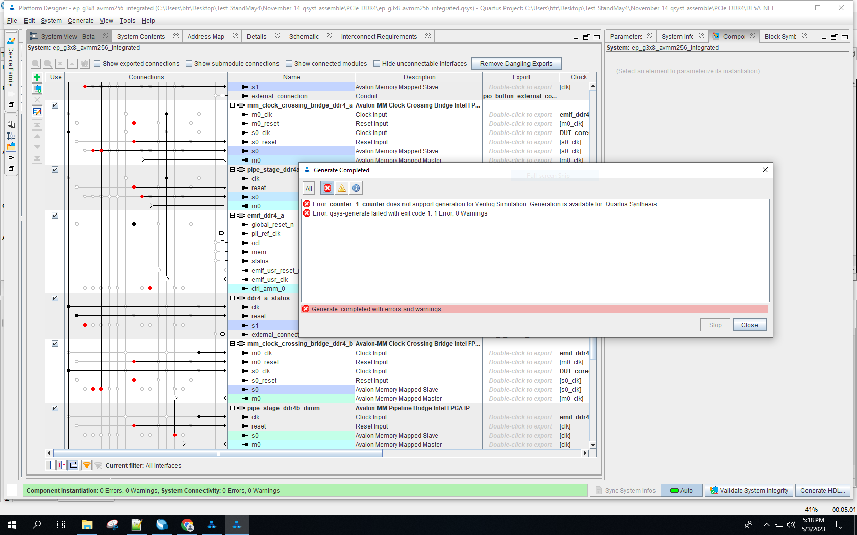
2) Used DE5A_NET.qpf as my quartus project file and opened it in Quartus Prime Pro. Then launched Platform Designer System and opened the ep_g3x8_avmm256_integrated.qsys. Added Avalon FIFO IP and custom generated IP for the counter (of which verilog file file sent to you). Followed steps like System Sync Info, Validate System Integrity and generating HDL. When I turn on the simulation option in the Generate HDL GUI (turn on means selecting VHDL/Verilog option. Turned off means selecting none for the simulation option and keeping just ) I gets some error (attached error_simulation.PNG). But when just Synthesis option= Verilog and simulation= none, no error. I am aware that this is something related to counter code which is synthesis-able only. Do you have any suggestion regarding how to make a custom IP out-of counter.v code that is compatible for both synthesis and simulation?
Schematic view of the modified ep_g3x8_avmm256_integrated (pls see file block_symbol_file.pdf ) is attached to see how the new components are added to the existing ep_g3x8_avmm256_integrated
3) I assume the Generate HDL option instantiates IP's and verilog code for individual design components?. Also in PCIe/DDR4/ep_g3x8_avmm256_integrated/synthesis we gets an updated verilog file with all components of the design ep_g3x8_avmm256_integrated.v (I have e-mailed this file) .
4) Then I came back quartus project DE5A_NET.qpf and added counter.v to the project. We can see ep_g3x8_avmm256_integrated.v is listed under ep_g3x8_avmm256_integrated.qsys in the quartus project (please see Image1.PNG and Image2.PNG).
5) The pin assignment is not needed as my modified design does not have any additional external interface that should be assigned (just kept whatever assigned by default). This project compiles fine (keeping DE5A_NET.v as a top-level entity) and it takes ~30 mins to finish. Using the DE5A_NET.sof file created in PCIe_DDR4/output_files, I have programmed the FPGA board. But when trying to access the data from the host PC using DMA Read API, I am getting same result (Capture2.PNG) as I mentioned in my message on dated 04-17-2023. Please note that even-though I have modified my counter code, I am getting something similar to what I got earlier.
6) On this ground, I am bit confused that any modification that I have to do explicitly in the DE5A_NET.v (which is taken as my top-level design entity)?. I would like to know whether the changes I made in Platform Designer System (here modified ep_g3x8_avmm256_integrated.qsys) will get into DE5A_NET.v?. If so could you explain how that happens?
{Or I have to use ep_g3x8_avmm256_integrated/sysnth/ep_g3x8_avmm256_integrated.v as top-level entity?. I would like to report that, when I try set as "top-level entity entity" option on this in Platform Designer ->Project Navigator->Files, the top-level entity label is visible on ep_g3x8_avmm256_integrated.qsys instead of ep_g3x8_avmm256_integrated/sysnth/ep_g3x8_avmm256_integrated.v. (I am curious that its due to ep_g3x8_avmm256_integrated/sysnth/ep_g3x8_avmm256_integrated.v has some dependency to ep_g3x8_avmm256_integrated.qsys in Platform Designer ->Project Navigator->Files?). Also from your last reply, I understood that I cannot use ep_g3x8_avmm256_integrated.qsys as my top-level entity.
I tried adding ep_g3x8_avmm256_integrated.v directly to the project (not like as a component under ep_g3x8_avmm256_integrated.qsys by default. For this I just copied the file to the project directory and set it as top-level entity and compiled). All these gives error Capture3.PNG.}
Please let me know if anything is missing or I did something that I am not suppose to do to get a modified design (Counter + FIFO + PCIe DMA transfer example design) working. I have emailed you the files DE5A_NET.v , ep_g3x8_avmm256_integrated.qsys , counter.v ,ep_g3x8_avmm256_integrated.v, hoping these may be helpful for you to address my questions.Thank you very much.
- Mark as New
- Bookmark
- Subscribe
- Mute
- Subscribe to RSS Feed
- Permalink
- Report Inappropriate Content
Hi Sijith,
From my understanding, this project has a top level entity as DE5A_NET. Inside the DE5A_NET.v, the ep_g3x8_avmm256 module is included.
That means every change in the ep_g3x8_avmm256.v will reflect in project.
Because the current issue is we want to confirm that the data is written into the memory, I may suggest you to create an EMIF example design and include the rtl code for counter part.
The EMIF example design will include a traffic generator module that will control the Read and Write transaction.
Regards,
Adzim
- Mark as New
- Bookmark
- Subscribe
- Mute
- Subscribe to RSS Feed
- Permalink
- Report Inappropriate Content
Hi Adzim,
Thank you very much for your reply. I have Emailed you my working directory PCIe_DDR4 which contains all files related to the project.
1) Before, I was doubtful whether the top-level entity DE5A_NET.v is getting updated when the the ep_g3x8_avmm256.v is updated with new design (automatically from modification in Platform Designer System). I got this doubt because the DE5A_NET.v did not change after I modified the .qsys file in the Platform Designer System (In other words,the DE5A_NET.v with just PCIe DMA example design is exactly the same even when I add counter and FIFO IP with the PCIe DMA example design).
But from your reply I assume that even if nothing changed in DE5A_NET.v, the included ep_g3x8_avmm256 module maps the ep_g3x8_avmm256.v and so whatever changes ep_g3x8_avmm256.v have reflected in DE5A_NET.v?
2) If I create an EMIF example design and include the rtl code for counter part, how I can view from my host system that the data is getting written there? Is there any provision in the EMIF example design? Could you elaborate it bit more?
3) Any comment regarding point 2 of my last message..... "When I turn on the simulation option in the Generate HDL GUI (turn on means selecting VHDL/Verilog option. Turned off means selecting none for the simulation option and keeping just ) I gets some error (attached error_simulation.PNG). But when just Synthesis option= Verilog and simulation= none, no error. I am aware that this is something related to counter code which is synthesis-able only. Do you have any suggestion regarding how to make a custom IP out-of counter.v code that is compatible for both synthesis and simulation? "
- Mark as New
- Bookmark
- Subscribe
- Mute
- Subscribe to RSS Feed
- Permalink
- Report Inappropriate Content
Would like to add a couple of lines to the point-2 of my last message. I assume you were suggesting me to use my counter IP and FIFO IP and attach to EMIF IP to check?Or something else? great if you could elaborate the process. Also is it possible for me to monitor the data transferred to DDR4? Thank you very much.
- Mark as New
- Bookmark
- Subscribe
- Mute
- Subscribe to RSS Feed
- Permalink
- Report Inappropriate Content
Hi Sijith,
I am not received the email that you have sent. Can you send it through Private Message then?
I will ping you there.
1) But from your reply I assume that even if nothing changed in DE5A_NET.v, the included ep_g3x8_avmm256 module maps the ep_g3x8_avmm256.v and so whatever changes ep_g3x8_avmm256.v have reflected in DE5A_NET.v?
- Yes the top level design should call all module within it.
2) If I create an EMIF example design and include the rtl code for counter part, how I can view from my host system that the data is getting written there? Is there any provision in the EMIF example design? Could you elaborate it bit more?
- To view the data, you can use Signal Tap tool and monitor the signals from example design.
- There is a Traffic Generator module that act as user logic controller.
- You can monitor the signals from this module to check on read data after the read transaction has been performed.
3) Do you have any suggestion regarding how to make a custom IP out-of counter.v code that is compatible for both synthesis and simulation?
- I think it's better to have another thread for checking on this issue. Then the expertise will come to help on this issue.
Regards,
Adzim
- Mark as New
- Bookmark
- Subscribe
- Mute
- Subscribe to RSS Feed
- Permalink
- Report Inappropriate Content
Hi Adzim,
It would be great if you ping me with the private email to send files. But for now, I would like to attach here the compressed folder contains my working directory regarding the integration of custom IP and FIFO with the DMA transfer example design. (it have counter.v in the directory and top-level DE5A_NET.v and all related files. just removedep_g3x8_avmm256_integrated_tb folder to reduce size.)
1) I assume that since ep_g3x8_avmm256 module have instantiations of FIFO IP and Counter, we don't need them to instantiate in the top-level module DE5A_NET.v, right?
2) Would be great if you could have a look in the g3x8_avmm256_integrated.qsys file in the platform designer system to see interface connections I used. Also great if you could have a look into my counter.v too.
3) I am curious that if our counter IP (through FIFO IP) could write to DDR4 in EMIF example design, then the counter IP should be able to write in the DDR4 of the PCIe DMA transfer example design? {Is there any chance for the components in the PCIe DMA transfer example design which the EMIF example design example does not have will have any effect in the data transfer to DDR4} or your suggestion is just to check if the counter IP is capable of streaming data?
Thank you.
- Mark as New
- Bookmark
- Subscribe
- Mute
- Subscribe to RSS Feed
- Permalink
- Report Inappropriate Content
Hi Adzim,
1) As you suggested in our last meeting, I was trying to map the memory map slave address to the Base Address (the address value specified in the PCIe DMA example design API Code. To access the DDR4 A, the starting address specified in API was 0x20000000 with a size of 4GB (I assume, it means the address span is from 0x20000000 to 0x30000000?) , and for DDR4 B the address specified was 0x40000000 with 4GB size). But unfortunately, I could not succeeded in it as I was bit unclear about the place to put the address in the code. It would be great if you could help me in that. Also, I would like to make sure the code where we should do changes is in the PCIe_DDR4/ip/ep_g3x8_avmm526_integrated_fifo_9 folder (As shown in attachment Fifo_slaveaddress1.PNG)?
2) I am wondering that is it possible to set the slave address parameter in the Platform Designer System (In the address space shown in attachments Addressmaps.PNG or Addressmap1.PNG) . If we can do it, when I was trying it I faced a difficulty: - {When I tried to change the adress maping of Avalon Memory map Slave address of "avalon fifo" component in Platform Designer (Addressmap1.PNG), I could change the address in the "Base" colum, but the corresponding "end" colum entry cannot change. Did I miss something that disable me to change it? (I was looking for a option in parameter editor in the Avalon FIFO IP, but could not see an option for it) }.
3) I have a additional question for you, parallel to this I was just trying to simulate my counter Custom IP + Avalon FIFO IP to see the correct data wave form is getting out of this design (I could get a waveform out of counter.v code in the modelsim simulator). But I am confused how I can simulate it when have I have them in the Platform Designer as IP's. I remember you mentioned me you did simulate the counter+EMIF Example design. It would be great you could mention how to do it (or any link that can help?). I could not find any RTL simulation tool in my Quartus Prime Pro. What I was trying to do is, a) After generating HDL and generating testbench, b) Executed `Generate simulation for IP`, I assume it generates simulation files in the project directory?. c) Then I tried to open a new IntelFPGA modelsim project and added all verilog codes (corresponding to all components) from the ip/<component_name>/synth folder of my project to it and try to run it. But I assume this is not what we are suppose to do?
Thank you very much and please let me know if you have any question.
- Subscribe to RSS Feed
- Mark Topic as New
- Mark Topic as Read
- Float this Topic for Current User
- Bookmark
- Subscribe
- Printer Friendly Page