- Mark as New
- Bookmark
- Subscribe
- Mute
- Subscribe to RSS Feed
- Permalink
- Report Inappropriate Content
Hello,
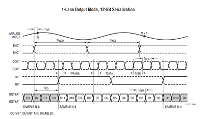
I am trying to connect 8 4-channel ADC to an Arria 10 FPGA. The ADC (LTC2171-12) has 4 differential LVDS pairs as well as one LVDS pair for the frame clock and one pair for the data clock.
The target is to reach a data rate of 360 Mbps. The image above shows, that the data output is in double data rate.
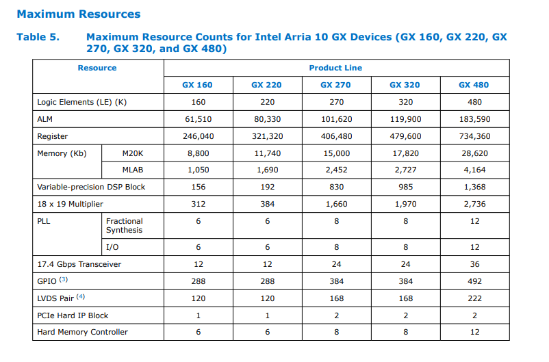
The Arria 10 GX270 has a maximum of 8 IO PLL and 8 FPLL in the F29 package. It has 2 transceiver banks as well as 8 IO banks. One of these IO banks is capable of 3V (bank 2L).
I am trying to use the Intel LVDS SERDES IP core for this case.
When I try to instantiate 8 instances of the SERDES and put the clock inputs of 2 instances in the same bank the fitter gives me an error, because it can't place 2 PLL in the same bank. When I spread the 8 SERDES over the 8 banks the fitter also gives me an error, because the LVDS clock and data inputs can't be placed in the 3V bank.
Is that correct? Is there any way to place 8 SERDES in an Arria 10 that has 8 IO banks and 8 IO PLL?
I have not found a setting for DDR in the SERDE IP core. I have set the "Data rate" field to "360" and the "Desired inclock frequency" to "180".
Is that the correct way to achieve double data rate with the SERDES IP core?
The ADC has bit depth of 12, which can be seen in the image above. To achieve this I wanted to set the "SERDES factor" to 12, but 10 is the maximum. My next guess was to set it to 6 and then later put it together in FPGA logic.
Is that the correct way to achieve a SERDES factor of 12?
I have also seen FPGA designs that interact with similar multi channel ADC by just passing the data clock through a PLL and then sampling the data signals with this clock and a ALTDDIO component. That was implemented in a Cyclone IV FPGA - the ALTDDIO doesn't exist for the Arria 10 (at least in the Quartus 19.1 Standard Edition).
I have already tested to instantiate 8 PLL in the design (the clock input of one PLL had to be put to a high speed transceiver pin, because of the 3V bank) and it worked out.
What would be the alternative to the ALTDDIO IP core for an Arria 10? Is it even ok to put the PLL clock to the transceiver pin? I was able to see that the IO PLL of bank 2L (3V bank) was used in this case.
Originally I wanted to use an Arria 10 GX160, but then migrated to the GX270 because of the 8 IO PLL, but at the moment it seems like only the GX480 and upwards with its 12 IO PLL can fit the desired design. Regarding all other constraints, first of all cost, the GX480 would be a terrible choice.
Best regards,
Florian
Link Copied
- Mark as New
- Bookmark
- Subscribe
- Mute
- Subscribe to RSS Feed
- Permalink
- Report Inappropriate Content
Hello Florian,
This is to let you know that I am investigating your request. Please give me sometime to get the solution for your request.
regards,
Farabi
- Mark as New
- Bookmark
- Subscribe
- Mute
- Subscribe to RSS Feed
- Permalink
- Report Inappropriate Content
Hello,
Yes, you may have issues on resource availability for your implementation.
Referring to below table, IOPLL for your implementation would take bigger size of Arria 10 device.
However, you may take advantage of the transceiver resources to implement LVDS if the IOPLL is not enough.
regards,
Farabi
- Mark as New
- Bookmark
- Subscribe
- Mute
- Subscribe to RSS Feed
- Permalink
- Report Inappropriate Content
Hello,
I’m glad that your question has been addressed, I now transition this thread to community support. If you have a new question, feel free to open a new thread to get the support from Intel experts. Otherwise, the community users will continue to help you on this thread. Thank you.
regards,
Farabi
- Subscribe to RSS Feed
- Mark Topic as New
- Mark Topic as Read
- Float this Topic for Current User
- Bookmark
- Subscribe
- Printer Friendly Page

