- Mark as New
- Bookmark
- Subscribe
- Mute
- Subscribe to RSS Feed
- Permalink
- Report Inappropriate Content
We are using the EP3C55 Cyclone III FPGA in our design. I have a query regarding the VCCIO for a bank when using LVDS IO.
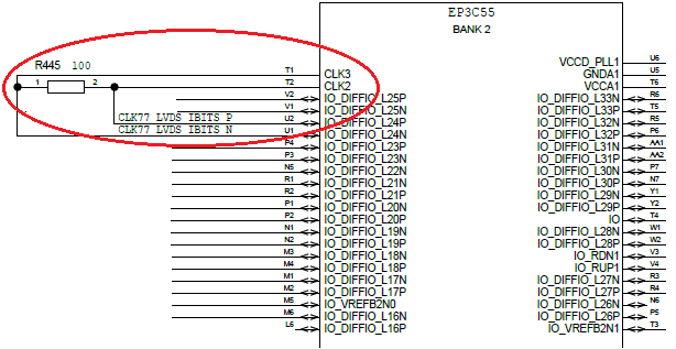
Here on Bank 1 and Bank 2, we have taken an LVDS clock output and connected to LVDS clock input.
The reason for looping back LVDS output to LVDS input is: In our design MSB outputs of four single-phase NCOs are combined using the Altera LVDS serializer to generate the 680 MHz resolution output clock (Output clock frequency is 77.76MHz and 77.2MHz)
In our design we have a requirement to connect the remaining IOs in the bank 1 and 2 to 1.8V IO interfaces due to which we require the VCCIO to be 1.8V.
· I would like to know if there is an issue if we connect the VCCIO for these banks to 1.8V instead of 2.5V and still configure the clock IO as LVDS? If there is an issue, please let me know which specification gets violated and how it impact the LVDS Output /Clock input buffer?
· Is there any workaround to enable using the LVDS Output and Clock input buffer in the Bank and still have the VCCIO at 1.8V?
As per AN 479: Design Guidelines for Implementing LVDS Interfaces in Cyclone Series Devices
Bank VCCIO level for LVDS inputs and outputs: LVDS input and output must be powered with a 2.5-V VCCIO supply in the banks where it resides, except for the following conditions in which a 2.5-V VCCIO supply is not required:
■ All LVDS inputs for the Cyclone device are powered by VCCINT
■ All LVDS dedicated clock inputs for Cyclone II are powered by VCCINT
Supplying higher than supported voltage to VCCIO for LVDS violates the rated specifications and may damage the buffer.
· From the Cyclone III datasheet, the VICM min is 0.05V which I hope should not be an issue if 1.8V VCCIO is used.
Link Copied
- Subscribe to RSS Feed
- Mark Topic as New
- Mark Topic as Read
- Float this Topic for Current User
- Bookmark
- Subscribe
- Printer Friendly Page

