- Mark as New
- Bookmark
- Subscribe
- Mute
- Subscribe to RSS Feed
- Permalink
- Report Inappropriate Content
Hi all,
I create this thread because I have a debug problem. On my PCB, my FPGA (EP3C5E144C8N) has to generate a clock to a PHY chip (Marvell 88E1111). With my scope, I can see this clock at 125MHz as expected but the '0' is 800mV and the '1' is 1.6V, rather than the 0v and 2.5V expected. The voltage level I saw on the scope doesn't respond to the spec (threshold for detection of a '0' or '1') of the PHY chip, so I can't establish communication between my system and my PC. The concerned bank has correct VCCio (2.5V precisely), the FPGA doesn't exceed the consumption which my regulator can give, I don't see false contact. Everything seems perfect because other bank makes what the programm wants. I have no more idea :confused:. PLEASE HELP Thanks in advance hinanotabu86Link Copied
11 Replies
- Mark as New
- Bookmark
- Subscribe
- Mute
- Subscribe to RSS Feed
- Permalink
- Report Inappropriate Content
Check the IO-standard and drive strength for the output.
Isn't the standard set to differential (LVDS), by accident? Cheers, Ton- Mark as New
- Bookmark
- Subscribe
- Mute
- Subscribe to RSS Feed
- Permalink
- Report Inappropriate Content
thanks std_logic_vector
my IO standrd is 2.5V, pin planner proposed me 2.5V or 2.5V(default), I choose 2.5V without suffix It isn't differential Vccio of the bank is exactly 2.51V Any others idea guys ?- Mark as New
- Bookmark
- Subscribe
- Mute
- Subscribe to RSS Feed
- Permalink
- Report Inappropriate Content
hi again,
does someone know if there is lots of difference of output current on pins between EP3C5E144C8N the one I use and the EP3C120F780C5N the one where my development project which works in the past ? Maybe someone can tell me where I can search, because in the Cyclone III handbook, it seems that there is no difference between all cyclone III concerning output current on pins thanks in advance hinanotabu86- Mark as New
- Bookmark
- Subscribe
- Mute
- Subscribe to RSS Feed
- Permalink
- Report Inappropriate Content
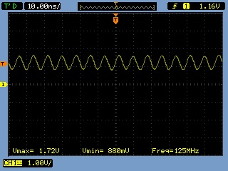
So I had some spare time and did some experiments. I made a 125MHz output with 8mA drive strength and 24mA drive strength,
both with and without the attribute "fast output register" on and off. I noticed little or no difference. But what made a big difference was the way that I measured the signal. With an x1 probe, I got the same result as hinanotabu86, with an x10 probe, the signal levels looked alot better. See attachment. This is a 3V3 output pin. The scope has a B/W of 200 MHz. Same scale for both signals. For the x1 probe (green): Vmin = 800 mV, Vmax = 2V. For the x10 probe (yellow): see scope picture. So I think your signal is fine, but the way you measure it should be improved. Good luck with your project, Ton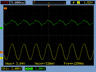
- Mark as New
- Bookmark
- Subscribe
- Mute
- Subscribe to RSS Feed
- Permalink
- Report Inappropriate Content
thanks std_logic_vector
incrdible similarity, in my case the clock is a nice sinusoide but with bad voltage level i checked pin planner, my clock pin is 2.5V (no suffix), nothing concerning LVDS (a colleage suggest me that) the corresponding bank has a correct voltage supply VCCio to 2.5V / GND to 0V, and I have separate the 2.5V supply for numeric and the 2.5V for analog no other ideas ? thanks in advance in my point of view the shape of signal is correct but can't be detected by the PHY chip, because no communication between my prototype and the PC- Mark as New
- Bookmark
- Subscribe
- Mute
- Subscribe to RSS Feed
- Permalink
- Report Inappropriate Content
- Mark as New
- Bookmark
- Subscribe
- Mute
- Subscribe to RSS Feed
- Permalink
- Report Inappropriate Content
lots of people told me about an impedance adaptation
considering that i can't recompile my project (because of a licence of one particular IP I bought), does someone know how to adapt impedance without an operationnal amplifier- Mark as New
- Bookmark
- Subscribe
- Mute
- Subscribe to RSS Feed
- Permalink
- Report Inappropriate Content
Hi all
The problem still occurs on my prototype Here is today's diagnosis : - The track has a length of 2cm. And in comparision whit datasheet, it doesn't seem to be an impedance adaptation problem - I try on another prototype card, still unsuccesfull - I cut the track just in front of the concerned pin, the clock stay between 0.7V and 1.8V - The board is correctly routed, no false contact and all power (VccIO, VccInt, GND) have the good voltage - Someone suggest me that the concerned pin has an special function "VREFB3N0", but i don't think that's a problem - another tell me that another clock, which stay inside the FPGA, is a virtual clock, but on the dev board with the same programm it wasn't a problem finally my prototype still not working but why ? and how solve that ? Thanks for any suggestions to unblock my situation hinanotabu86- Mark as New
- Bookmark
- Subscribe
- Mute
- Subscribe to RSS Feed
- Permalink
- Report Inappropriate Content
Hi hinanotabu86,
Actually the use of a VREF pin could be the problem. VREF pins have a higher capacitance than normal pins. With a frequency of 125MHz this certainly has (some) impact. From the Cyclone III handbook: When VREF pins are used as regular I/Os, they have higher pin capacitance than regular user I/O pins. This has an impact on the timing if the pins are used as inputs and outputs. From the Cyclone III datasheet:When VREF pin is used as regular input or output, a reduced performance of toggle rate and tCO is expected due to higher pin capacitance. The capacitance of the VREF pin is 21 or 23 pF. For a normal pin it's about 6 pF. Just route your output to another pin, and measure again. Just to be sure Good luck, Ton- Mark as New
- Bookmark
- Subscribe
- Mute
- Subscribe to RSS Feed
- Permalink
- Report Inappropriate Content
hi std_logic_vector
thanks for information The problem on my prototype is taht i can't compile again, for rerouting the pcb, i have to wait three weeks for a new one nevertheless, i verify the same clock on my dev board where the communication works well, the same clock (on a VREF pin too) has exactly the same caracteristic, so i begin to get crazy whith this problem someone told me about the schematics around the PHY chip^, i'll work on this way today thanks again for help hinanotabu86- Mark as New
- Bookmark
- Subscribe
- Mute
- Subscribe to RSS Feed
- Permalink
- Report Inappropriate Content
How did you measured that sinusoidal waveform? What scope and what probe were used? What was probe divider?
Reply
Topic Options
- Subscribe to RSS Feed
- Mark Topic as New
- Mark Topic as Read
- Float this Topic for Current User
- Bookmark
- Subscribe
- Printer Friendly Page