- Mark as New
- Bookmark
- Subscribe
- Mute
- Subscribe to RSS Feed
- Permalink
- Report Inappropriate Content
hi,
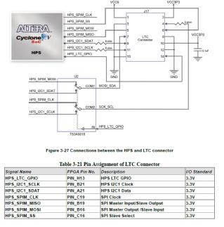
i am using quartus to connect a DAC daughter board to de0 nano soc through LTC connector. i am using i2c protocol.but when i do the pin assignments , its saying that ""value entered is not a valid location" . i am trying to connect i2c_sda to PIN_A21 & i2c_scl to PIN_B21 in pin planner my module initiation ismodule fpga_i2c(
input clk,input reset,input i2c_select,inout reg i2c_sda,output wire i2c_scl ); pin assignment table manual ltc connector is describe in de0_nano_soc user manual page 41. after thiis i tried with assignment editer. then i am able to assign the pins. but when i complied it it generated follwing error
Error (14566): The Fitter cannot place 2 periphery component(s) due to conflicts with existing constraints (2 pin(s)). Fix the errors described in the submessages, and then rerun the Fitter. The Altera Knowledge Database may also contain articles with information on how to resolve this periphery placement failure. Review the errors and then visit the Knowledge Database at https://www.altera.com/support/support-resources/knowledge-base/search.html and search for this specific error message number.    Error (175020): The Fitter cannot place logic pin in region (60, 61) to (60, 61), to which it is constrained, because there are no valid locations in the region for logic of this type.
        Info (14596): Information about the failing component(s):
            Info (175028): The pin name(s): i2c_scl
        Error (16234): No legal location could be found out of 1 considered location(s).  Reasons why each location could not be used are summarized below:
            Error (184016): There were not enough single-ended output pin locations available (1 location affected)
                Info (175029): B21
            Info (175015): The I/O pad i2c_scl is constrained to the location PIN_B21 due to: User Location Constraints (PIN_B21)
                Info (14709): The constrained I/O pad is contained within this pin
    Error (175020): The Fitter cannot place logic pin in region (60, 61) to (60, 61), to which it is constrained, because there are no valid locations in the region for logic of this type.
        Info (14596): Information about the failing component(s):
            Info (175028): The pin name(s): i2c_sda
        Error (16234): No legal location could be found out of 1 considered location(s).  Reasons why each location could not be used are summarized below:
            Error (184016): There were not enough single-ended bidirectional pin locations available (1 location affected)
                Info (175029): A21
            Info (175015): The I/O pad i2c_sda is constrained to the location PIN_A21 due to: User Location Constraints (PIN_A21)
                Info (14709): The constrained I/O pad is contained within this pin
Error (12289): An error occurred while applying the periphery constraints. Review the offending constraints and rerun the Fitter.
i wanted to connect a dac daughter board to de0 nano soc through LTC connector using i2c interface. after that need to send a 32 bit data(as specified in 2607 manual) to dac and read the voltage on output.i am using LTC 2607 as daughter board. can anybody help me on this issue. thanks and regards
Link Copied
1 Reply
- Mark as New
- Bookmark
- Subscribe
- Mute
- Subscribe to RSS Feed
- Permalink
- Report Inappropriate Content
It looks like you're trying to connect your own logic to dedicated HPS pins on the FPGA. These signals are intended for the HPS to host an I2C bus. So, it's not as straightforward as simply constraining your design in the way, I suspect, you have.
You can connect your own logic to these HPS signals. Refer to an 706: mapping hps ip peripheral signals to the fpga interface (www.altera.co.uk/literature/an/an706.pdf) for details of what you can do. Cheers, Alex
Reply
Topic Options
- Subscribe to RSS Feed
- Mark Topic as New
- Mark Topic as Read
- Float this Topic for Current User
- Bookmark
- Subscribe
- Printer Friendly Page