- Mark as New
- Bookmark
- Subscribe
- Mute
- Subscribe to RSS Feed
- Permalink
- Report Inappropriate Content
Hello there,
I have a Texas Instruments module that outputs ADC data using 4-lanes LVDS from its Mezzanine connector. It provides LVDS_CLK and LVDS Frame Clock alongwith. I want to receive this data using HSMC of Intel FPGA (possibly Stratix IV) and do some processings. Could you have a look into the details I am providing below for the two systems - TI module and Intel FPGA - and comments if I may run into some issues, like synchronization?
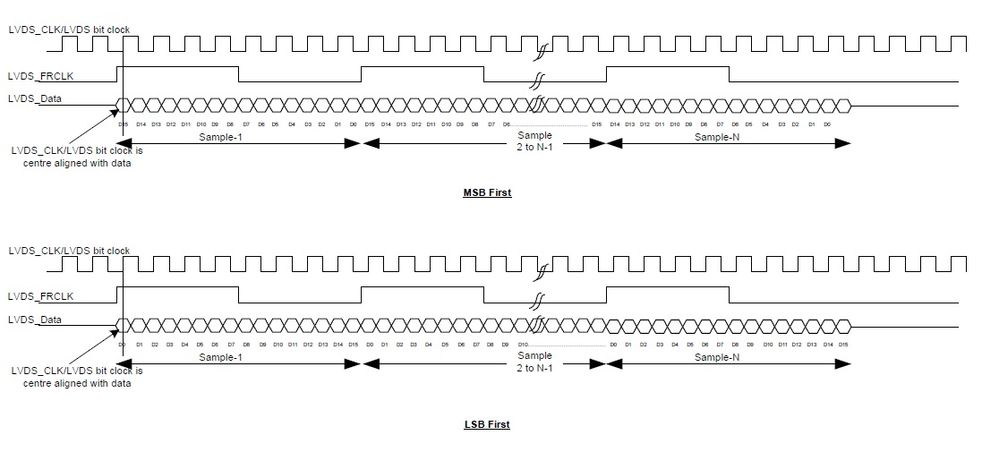
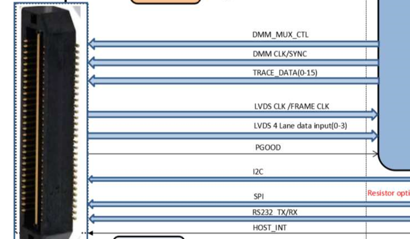
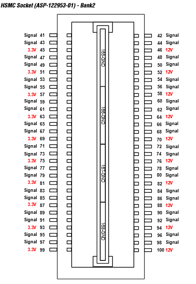
1. The pin mapping of TI Mezzanine and LVDS part of HSMC are different. I've attached the timing diagram of TI module LVDS output and the pin diagrams for both. So a custom PCB that performs proper mapping of clock and data lanes would make them compatible, right? Also, is Frame Clock required for receiving data into HSMC? I didn't see it being used in the LVDS Rx fabric of Intel FPGA.
2. I don't have much control on the ADC samples output configuration, except from data rate, from the TI module. I should be able to receive the data from two lanes synchronously using Intel FPGA IP, or there are some potential problems?
I would highly appreciate detailed comments :)
Best,
Arvind
- Tags:
- Stratix® IV FPGAs
Link Copied
- Mark as New
- Bookmark
- Subscribe
- Mute
- Subscribe to RSS Feed
- Permalink
- Report Inappropriate Content
Hi
1. The pin mapping of TI Mezzanine and LVDS part of HSMC are different. I've attached the timing diagram of TI module LVDS output and the pin diagrams for both. So a custom PCB that performs proper mapping of clock and data lanes would make them compatible, right?
==> yes
Also, is Frame Clock required for receiving data into HSMC?
==> Frame Clock is required.
I didn't see it being used in the LVDS Rx fabric of Intel FPGA.
==> Frame clock is the naming for ADC. LVDS RX IP is a generic IP...expected that your frame clock is connected to the rx_inclock.
2. I don't have much control on the ADC samples output configuration, except from data rate, from the TI module. I should be able to receive the data from two lanes synchronously using Intel FPGA IP, or there are some potential problems?
==> it seems to me that you have 4 lanes of data (not 2 lanes)
- Subscribe to RSS Feed
- Mark Topic as New
- Mark Topic as Read
- Float this Topic for Current User
- Bookmark
- Subscribe
- Printer Friendly Page


