- Mark as New
- Bookmark
- Subscribe
- Mute
- Subscribe to RSS Feed
- Permalink
- Report Inappropriate Content
Hello,
According to Intel LPC specification (ver. 1.1 from 2002, document number : 251289-001) the LPC bus clock is 33Mhz (page 9, signal LCLK), but in the PCH 300 series (QM370) it is 24MHz measured with scope on the PCB.
According to the PCH 300 series datasheet vol. 1 (Doc number : 337347-004) in page 184, 24.7 Functional Description is written:
"The PCH LPC interface supports the Low Pin Count Interface Specification. The bus operates at 24MHz clock frequency."
The PCH datasheet vol. 1 refer to LPC bus specification 1.1 in the page 183, 24.3.
Anybody to know if Intel has newer version of the LPC bus specification where clock frequency was changed?
Best Regards,
Krasimir Kostadinov
Link Copied
- Mark as New
- Bookmark
- Subscribe
- Mute
- Subscribe to RSS Feed
- Permalink
- Report Inappropriate Content
Hello, @knk@xpeqt.com:
Thank you for contacting Intel Embedded Community.
In order to be on the same page, could you please clarify if this clarification is related to a technical problem? Please give us all the details of the issue in case that your answer is affirmative.
Waiting for your answer.
Best regards,
- Mark as New
- Bookmark
- Subscribe
- Mute
- Subscribe to RSS Feed
- Permalink
- Report Inappropriate Content
Hello Maecenas,
Indeed, the question from my side was exactly in regard to a technical problem.
I already open an support ticket and close it later after receiving a hint that I should post a question into embedded community forum.
Here I will copy my initial information and questions which I asked:
Used PC : Adlink Express-CF-i7-8850H, Com Express Type 6
Used CPU : Core™ i7-8850H
Used PCH : QM370, DeviceID 0xA30C
Used bus : LPC
The problem in short:
We are using Intel LPC bus to communicate with Xilinx FPGA. Our HW and SW which is working with 2nd, 3rd and 5th generation CPU can not establish communication with the FPGA anymore.
What we found so far:
According Intel LPC specification (ver. 1.1 from 2002, document number : 251289-001)
we expect 33MHz clock for the LPC bus (page 9, signal LCLK), but in the reality it is 24MHz for used PCH.
According to the PCH 300 series datasheet vol. 1 (Doc number : 337347-004) in page 184, 24.7 Functional Description is written:
"The PCH LPC interface supports the Low Pin Count Interface Specification. The bus operates at 24MHz clock frequency."
The PCH datasheet vol. 1 refer to LPC bus specification 1.1 in the page 183, 24.3.
We changed the FW of our FPGA to support 24MHz as well, but the communication was not restored.
In the next step we attach a scope to the LPC bus to find out the data, transmitting from the PCH to the FPGA and we found the following:
- the START field (described in 251289-001, page 15) has value 0101 binary (Bits[3:0]) which is reserved according to the LPC specification. This field is generated when we map a memory address and start writing or reading data.
- the Cycle Type Bit (CYCTYPE) is 000 binary for I/O Read and 001 for binary for I/O Write, but we expect 010 binary for Memory Read and 011 binary for Memory Write when we use memory map.
By the way there is a typo in the page 185, doc number 337347-004 : both cycle type bit definitions are for Memory Read, there is no Memory Write).
Questions so far from our side:
- Is there a newer LPC specification which is available?
- What means the value 0101 binary in the START field?
- Where is described the mechanism of getting a memory address which should be set in the LPC Generic Memory Range? It is written "The LGMR memory decode range is 64KB in size and can be defined as being anywhere in the 4GB memory space. This range needs to be configured by BIOS during POST to provide the necessary memory resources." in the PCH datasheet, but in fact BIOS never set this address and we always have to find out which is the correct one.
- Why the read or write requests to a mapped memory (via ioremap) are translated to I/O read/write request on LPC bus?
Best Regards,
Krasimir Kostadinov
Software Engineer
Xpeqt Ltd.
- Mark as New
- Bookmark
- Subscribe
- Mute
- Subscribe to RSS Feed
- Permalink
- Report Inappropriate Content
Hello, @knk@xpeqt.com:
Thanks for your reply.
Based on the provided information, we would like to help you with your third-party device but only its manufacturer has the proper information to answer your questions.
Due to this fact, we suggest you use in order to help you use the channels listed at the following websites as a reference:
https://www.adlinktech.com/en/support.aspx
https://www.adlinktech.com/en/Contact_us_form.aspx
We hope that this information may help you.
Best regards,
- Mark as New
- Bookmark
- Subscribe
- Mute
- Subscribe to RSS Feed
- Permalink
- Report Inappropriate Content
Dear Maecenas,
We contact Adlink and we got answer for our question regarding to the BIOS settings.
However the first two and the last questions are not related to PCB manufacturer, but to Intel which is the manufacturer of the CPU, PCH and creator of the LPC bus.
The LPC bus frequency was changed by Intel in their 300 series PCH and this is against the own Intel LPC specification. This is not done by Adlink.
Writing data into memory map does trigger Start field value which is reserved according the LPC specification.
Kind Regards,
Krasimir Kostadinov
- Mark as New
- Bookmark
- Subscribe
- Mute
- Subscribe to RSS Feed
- Permalink
- Report Inappropriate Content
Hello, @knk@xpeqt.com:
Thanks for your update.
We can provide generic information to your third-party design that should be confirmed by its manufacturer because some devices have been customized.
The START values are stated in section 4.2.1.1, on page 15 of the Intel(R) Low Pin Count [LPC] Interface Specification {August 2002, Revision 1.1} document # 251289. It is important to let you know that all encodings marked as “Reserved” are reserved for future use as you can confirm in the cited section of the LPC Specification that can be found at:
https://www.intel.com/content/dam/www/program/design/us/en/documents/low-pin-count-interface-specification.pdf
The frequency change seems to be related to an architecture change. Please refer to the information stated on page 20 of the Skylake Platforms Design In Presentation document # 556527.
The information that may answer your last question is stated in the note of the Table 22-1, on page 166 of the Intel(R) 300 Series Chipset Family On- Package Platform Controller Hub External Design Specification [EDS] Volume 1 of 2 {February 2019, Revision 2.3} document # 566439.
These documents are accessible when you are logged into your Resource & Design Center (RDC) privileged account at the following websites:
http://www.intel.com/cd/edesign/library/asmo-na/eng/556527.htm
http://www.intel.com/cd/edesign/library/asmo-na/eng/566439.htm
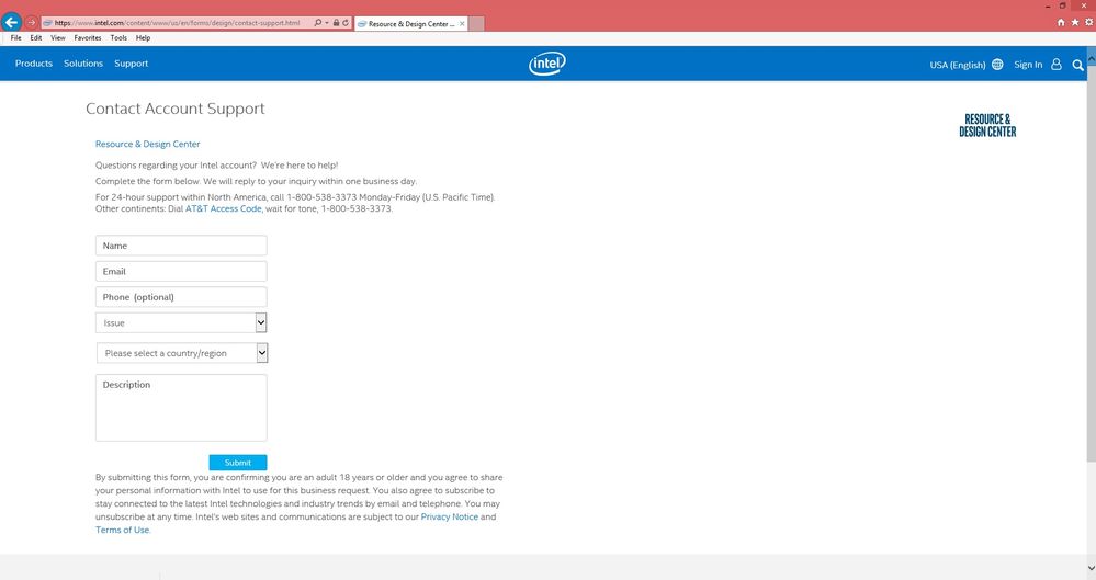
Your account can be upgraded by filling out the RDC Account Support form as is stated in the following website:
https://www.intel.com/content/www/us/en/forms/design/contact-support.html
Best regards,
- Mark as New
- Bookmark
- Subscribe
- Mute
- Subscribe to RSS Feed
- Permalink
- Report Inappropriate Content
Dear Maecenas,
Thank you for your input!
Unfortunately the page for upgrading to RDC account is not accessible.
Regards,
Krasimir Kostadinov
- Mark as New
- Bookmark
- Subscribe
- Mute
- Subscribe to RSS Feed
- Permalink
- Report Inappropriate Content
Hello, @knk@xpeqt.com:
Thanks for your update.
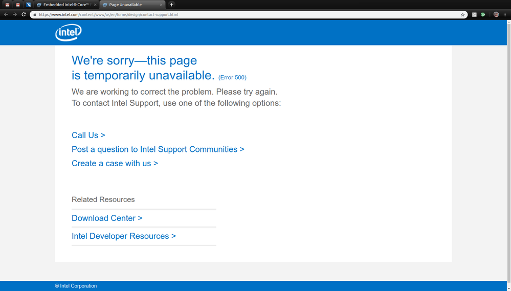
We have tried several times the provided website with the same result show at the following screenshot:
Due to this fact, could you please try again and let us know the results?
Waiting for your reply.
Best regards,
- Mark as New
- Bookmark
- Subscribe
- Mute
- Subscribe to RSS Feed
- Permalink
- Report Inappropriate Content
Hello,
I got again page unavailable error after clicking on provided link:
- Mark as New
- Bookmark
- Subscribe
- Mute
- Subscribe to RSS Feed
- Permalink
- Report Inappropriate Content
Hi again,
I was able to register. Waiting for approving.
- Mark as New
- Bookmark
- Subscribe
- Mute
- Subscribe to RSS Feed
- Permalink
- Report Inappropriate Content
Hello, @knk@xpeqt.com:
Thanks for your updates.
We are glad that your request has been processed.
Best regards,
- Mark as New
- Bookmark
- Subscribe
- Mute
- Subscribe to RSS Feed
- Permalink
- Report Inappropriate Content
Hello @knk
I know this is a topic from almost 4 years ago, but it appears that I've just run into what seems to be the same problem that you reported in this thread. I was wondering if you could share with me the details of the FPGA changes you had to make to be able to restore communication.
Regards,
Brendon
- Subscribe to RSS Feed
- Mark Topic as New
- Mark Topic as Read
- Float this Topic for Current User
- Bookmark
- Subscribe
- Printer Friendly Page

