Hello dlim,
I modified the custom Dipalyport Receiver board. The Modified point is CLKUSR pin only
DisplayPort Receiver function still doesn't work.
I attached two picture.
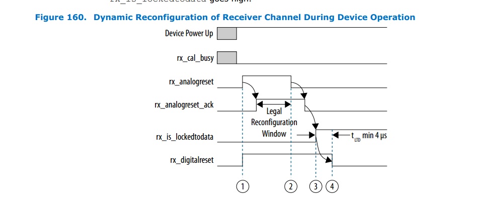
Picture 1 : cyclone 10gx transceiver PHY user Guide (20.1) page 259
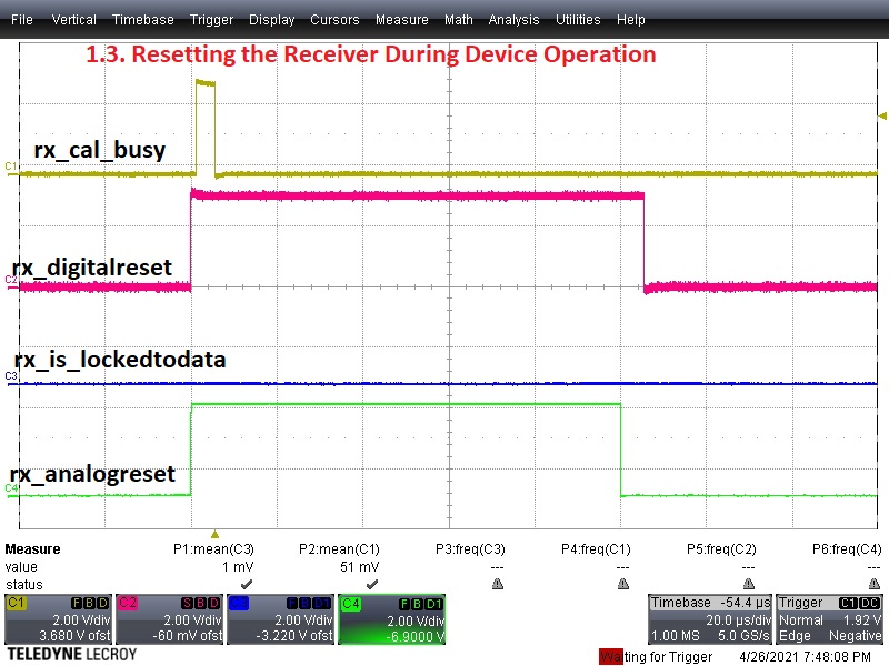
Picture 1: I probing from my board.
In my system, the rx_is_lockedtodata signal and rx_is_lockedtoref are always low (it is problem)
Can you advice how to make it to work ?
My concern is rx_cal_busy and rx_analogreset signal is overlapping (?)
I didn't change anything in bitec-reconfig_alt_c10.v and xcve_reconfig_arbiter.sv.
I checked all reconfiguration signals. it works good.
the calibration step works good because rx_analogreset asserted.
I think the PLL(rx_cdr_refclk0 : 135MHz) doesn't lock.
Michael
链接已复制
Hello dlim,
I attached two picture, it is for previous mail.
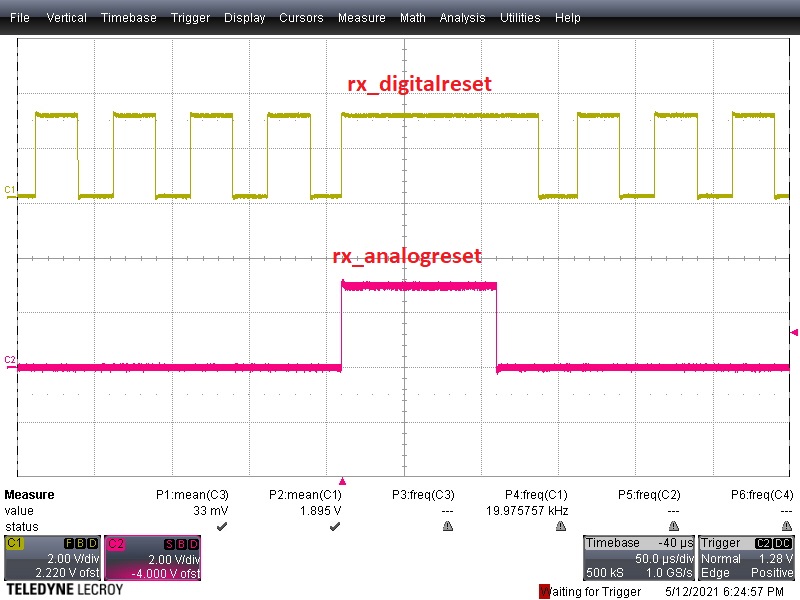
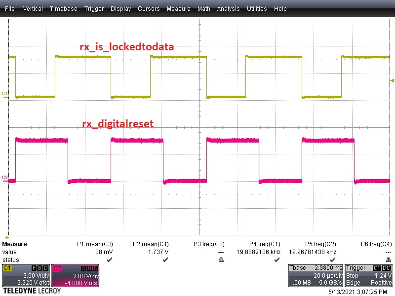
I captured all reconfiguration interface address and data. It looks correct.
The read and write operation repeated each channel but I captured only one channel.
I think the CDR pll doesn't lock. I checked 135MHZ clock. it is ok
Thanks
Michael
Attached is the C10 CDR loose lock debug check list for your reference
Hi,
ok, looks like transceiver calibration can be completed and it's not stuck in reset mode anymore
I have 2 suggestion for you. You should isolate whether the CDR loose lock issue is caused by your board issue or your Quartus design issue.
To rule out potential board issue :
- Perform FPGA transceiver channel internal loopback follow by external loopback on board
- FPGA transceiver channel internal loopback must works else there is really some issue with your board or the FPGA device itself or some manufacturing soldering contact issue
- You can perform internal loopback using transceiver toolkit. Reference design and user guide doc is available in below link
- https://fpgacloud.intel.com/devstore/platform/17.1.1/Pro/cyclone-10-gx-xcvr-toolkit-reference-design/
- Once you verified to get the internal loopback working, then you can move on to check with external loopback on your board. (assuming you can perform external loopback on your board)
- If it's failing with external loopback, then you can cross check the debug suggestion in CDR debug checklist that I shared with you in previous post
To rule out potential Quartus design issue
- It would be best if you can just stick with using DisplayPort Rx to Tx example design to bring up the DP Rx first before you move on to make design modification on it
Thanks.
Regards,
dlim
Hi dlim,
I installed C10GX_toolkit_demo design kit and I got same result as mine.
I probed internal signal as below
pll_locked : always "L" : means doesn't locked
locked : always " L" : this signal is IOPLL lock signal for test. but the 16MHZ clock comes out
rx_is_lockedtodata : always "L" : same result as my design
I attached C10GX_toolkit_demo design and Board schematic (power portion)
I think my board has a problem in PLL function and Power connection is correct or not (?)
Can you review where is wrong connection ?
Thank you
Michael
Hi Michael,
I am not power expert but I do noticed 2 main concern that alert me.
- FPGA RREF pins (Reference resistor for fPLL, IOPLL, and transceiver) is not connected to 2Kohm Resistor then to GND. Highly suspect PLL functionality failure is caused by RREF pins connection.
- FPGA Vref power supply pins : You may need to power up Vref pins depends on input IO pins usage (depends on IO standard)
It's very dangerous if there is still issue with your board design. I strongly recommend you to perform full board schematic review again. Below is one good reference doc that can help you on board schematic review
- https://www.intel.com/content/dam/www/programmable/us/en/pdfs/literature/dp/cyclone-10/pcg-01022.pdf
Thanks.
Regards,
dlim
RREF pin should be 2K Resistor.
You mean the VREFB (Input reference voltage) need to connect GND because I didn't use DDR3 and I use LVDS TX only (No need VREF voltage).
Can you explain more information for very dangerous issue ?
Does it mean the chip goes to HOT ?
(FPGA consumed total current is Max less 300mA, I think it is not much but I added the heatsink).
Thank you
Michael
Hi Michael,
By dangerous I mean if your board design connection is not done correctly then it may impact your FPGA design functionality.
For instance, does your board RREF pins has 2k resistor connection or not because I see RREF pins is floating in your pdf schematic ?
For VREF pin - the recommendation from C10 pin connection guideline doc that I shared with you is
- If VREF pins are not used, connect them to either the VCCIO in the bank in which the pin resides or GND
- You let VREF pin float which is not right but I think still fine.
- More important is did you use SSTL IO standard input pins for these IO bank or not ? If yes, then pls power up VREF pins accordingly else you can choose to connect VREF to VCCIO or GND
That's why I recommend you to review the C10 pin connection guildeline doc.
If everything is done correctly on your board design connection yet your ATX PLL in toolkit design still can't lock then you need to check following
- Ensure you are supplying correct clock frequency to ATX PLL refclk pin
- Ensure you provide the correct voltage swing as per the ATX PLL IO standard
Thanks.
Regards,
dlim
Hi
Thank you for recommending
I didn't use any voltage reference differcial IO. only 1.8V, 3.0V LVMOS and LVDS. So I will tie all VREF to GND. I didn't tie it to GND all other design I did before.
Thank you
Michael
Hi Michael,
Thanks for the update on VREF pins connection but anyway this is slightly off topic and VREF shouldn't impact DsiplayPort design.
Why not you focus back to debug on the transceiver refclk pin that's likely causing Rx CDR to loose lock issue ?
- Sorry but it's still not clear to me whether RREF pins is connected to 2k resistor on your board or not ?
- If NO then you need to fix it else if yes then you can try probe on transceiver refclk pin to check on the signal quality and also follow the C10 GX CDR debug guideline that I shared with you earlier
Thanks.
Regards,
dlim
Hello dlim,
I attached two picture and rx_analogreset, rx_digitalreset and rx_is_lockedtodata signal look good.
But still PC generate link failure (attached pic).
I think the failure is in DisplayPort link training sequence. I looked rx_reconfig read/write signal group and rx_link_rate_8bit appeared "14h, 0Ah, 06h. so PHY reconfiguration looks good.
Can you provide more information of DisplayPort link training sequence and aux channel access command to analyze problem ?
Any other check point do I need ?
Thanks
Michael
Hi,
out_dc, out_ac, out_vga is referring to transceiver Rx channel PMA parameter.
- For now you can just stick with default setting as set in DP example design
I looked at your screenshot, the transceiver behaviour is still not correct.
- Both rx_is_lockedtodata and rx_digital_reset keeps on toggling high and low instead of stay stable
- That means either DP link training keeps on failing and repeating causing transceiver to keeps on resetting or CDR itself keeps on loose lock and causing the transceiver to keeps on reset itself
You priority right now is to get CDR to lock stable and not toggling else if transceiver channel functionality is failing then DisplayPort won't work as well.
- Did you had a chance to use the transceiver toolkit design to perform internal loopback to check if CDR is locked ?
- If NO LOCK then something is seriously wrong. Pls check back the C10 Gx pin connection guideline doc
- If LOCKED then at least you know CDR is working within FPGA internal loopback
- Next if CDR is not locked during actual DP operation then likely it's due to board design connection or bad signal integrity issue
Side note : You can use Quartus signal tap tool to monitor the transceiver signal behaviour instead of doing on board probing
Once CDR is locked then you can dump MSA log using DP example design
- We can then find out more debug info from MSA log
It looks like you are still struggling a lot with your custom board.
- Do you want to consider to purchase C10 GX dev kit board + Bitec DP daughter card to aid in your issue debug ?
Thanks.
Regards,
dlim
Thank you for recommending.
I think to purchase C10 GX dev kit board + Bitec DP daughter card, There are many function so when I load my design, Board document doesn't show how to initialize state to avoid high current in unused pin in my design but kit board connected some part. so I can't use that kit board to verify my design. I just use circuit reference only.
I understood rx_is_lockedtodata signal behaver.
Since DP signal goes to FPGA through repeater chip (SN75DP130SSRGR) , it may be necessary to configure the repeater chip. I am not sure but I think the PC configured analog value of repeater chip through DPCD. so I didn't touch repeater chip register. If you have any information to control repeater chip (SN75DP130SSRGR), give me document.
Thank you
Michael
Hi,
Yup, Intel FPGA C10 GX dev kit board comes together with schematic and board layout file which should serve as good reference for your board design.
Regarding the control of repeater chip,
- I am sorry I don't have any doc for it as it's not Intel chip
- Reg configuration of repeater chip should be via DP example design NIOS software I2C bus design, not via DPCD but it's meaningless unless you download the the repeater datasheet to understand the repeater chip reg function
Thanks.
Regards,
dlim
Hi Michael,
Good news indeed !
So you are saying there is wrong DP signal assignment on your custom board ? Then you fixed it.
After that, is your custom board DP functionality working now ? or you still face some issue ?
Thanks.
Regards,
dlim
I removed the repeater chip control (using PIC Controller firmware : was blocked training sequence)
and DP rx_serial_input port was assigned reverse (But Still I can't understand)
Now my custom board works good.
My next concern is how to increase 8.1G data rate. There is no option in Non GPU DisplayPort mode (Max 5.4G)
Thank you
Michael
Hi,
Are you using very old Quartus version ?
- I do a quick check on v20.4 Quartus Pro and I can see that C10 GX FPGA DP IP did support till 8.1G.
The other thing to take note is for 8.1G (HBR3) support, it recommended to use repeater/retimer for DP Rx side. Checkout below link page 8, table 8
Thanks.
Regards,
dlim