- Mark as New
- Bookmark
- Subscribe
- Mute
- Subscribe to RSS Feed
- Permalink
- Report Inappropriate Content
I currently use the tiny bit of memory on the FPGA for a computer vision project but it's way too limited. I have a stand-alone SDRAM controller from Altera (partially pasted below) but I need one more layer above that which implements this controller as a 2-port RAM entity. It seems like overkill to use QSYS with NiosII though, plus I'm not very familiar with it. What's resource will help me implement this controller as a 2-port RAM entity in the simplest way possible?
entity sdr_sdram is
    generic(
        ASIZE     : integer := 23;
        DSIZE     : integer := 32;
        ROWSIZE   : integer := 12;
        COLSIZE   : integer := 9;
        BANKSIZE  : integer := 2;
        ROWSTART  : integer := 9;
        COLSTART  : integer := 0;
        BANKSTART : integer := 20
    );
    port(
        CLK     : in    std_logic;      --System Clock
        RESET_N : in    std_logic;      --System Reset
        ADDR    : in    std_logic_vector(ASIZE - 1 downto 0); --Address for controller requests
        CMD     : in    std_logic_vector(2 downto 0); --Controller command
        CMDACK  : out   std_logic;      --Controller command acknowledgement
        DATAIN  : in    std_logic_vector(DSIZE - 1 downto 0); --Data input
        DATAOUT : out   std_logic_vector(DSIZE - 1 downto 0); --Data output
        DM      : in    std_logic_vector(DSIZE / 8 - 1 downto 0); --Data mask input
        SA      : out   std_logic_vector(11 downto 0); --SDRAM address output
        BA      : out   std_logic_vector(1 downto 0); --SDRAM bank address
        CS_N    : out   std_logic_vector(1 downto 0); --SDRAM Chip Selects
        CKE     : out   std_logic;      --SDRAM clock enable
        RAS_N   : out   std_logic;      --SDRAM Row address Strobe
        CAS_N   : out   std_logic;      --SDRAM Column address Strobe
        WE_N    : out   std_logic;      --SDRAM write enable
        DQ      : inout std_logic_vector(DSIZE - 1 downto 0); --SDRAM data bus
        DQM     : out   std_logic_vector(DSIZE / 8 - 1 downto 0) --SDRAM data mask lines
    );
end sdr_sdram;
I need a wrapper so that this SDRAM controller is implemented like this: Inst_frame_buffer : entity work.sdram_wrapper_frame_buffer PORT MAP(
rdaddress => rdaddress, -- IN std_logic_vector(18 downto 0);
rdclock => clk_vga, -- IN std_logic;
q => rddata, -- OUT std_logic_vector(11 downto 0)
wrclock => camera_pclk, -- IN std_logic;
wraddress => wraddress, -- IN std_logic_vector(18 downto 0);
data => wrdata, -- IN std_logic_vector(11 downto 0);
wren => wren -- IN std_logic;
);
Link Copied
- Mark as New
- Bookmark
- Subscribe
- Mute
- Subscribe to RSS Feed
- Permalink
- Report Inappropriate Content
I began writing the simulation but when I wen to test it in modelsim, modelsim reported that it only supports one HDL. Since some of the files are verilog (generated by QSYS) it won't allow simulation.
I did get the SDRAM working but the display is mostly noise. I can tell it is somewhat working because the general color of the noise changes predictably as I aim the camera from a dark area to a bright area. The noise is likely because of issues with two masters fighting for access to the SDRAM chip. Also the sdram_controller_s1_waitrequest signal seems to be always high. 1. Is there possibly a required init period that I'm not allowing time for? 2. Is there a better way to delegate access to the SDRAM chip than what I'm doing below? Maybe alternate every other clock cycle? The SDRAM chip is made by ISSI. The pdf for this specific chip states that the acceptable clock frequencies are 133, 143, 166, & 200MHz. The altera tutorials that involve sdram instruct you to create a ALTPLL with a 50mhz output and a -3ns phase shift for the SDRAM. I was using a 100Mhz PLL with a -3ns phase shift. I'll try other frequencies. 3. Do you know what frequency I should be using? The information seems to be conflicting. sdram_controller : process(sdram_clk_s, btn(2))
begin
if btn(2) = '0' then
sdram_controller_s1_address_s <= (others => '0');
elsif rising_edge(sdram_clk_s) then
if (wren = '0') then
sdram_controller_s1_address_s <= rdaddress;
else
sdram_controller_s1_address_s <= wraddress;
end if;
end if;
end process;
SDRAM_BA_1 <= sdram_controller_wire_ba_s(1);
SDRAM_BA_0 <= sdram_controller_wire_ba_s(0);
SDRAM_UDQM <= sdram_controller_wire_dqm_s(1);
SDRAM_LDQM <= sdram_controller_wire_dqm_s(0);
SDRAM_ADDR <= '0' & sdram_controller_wire_addr_s(11 downto 0);
SDRAM_CLK <= sdram_clk_s;
wraddress(21 downto 19) <= (others => '0');
rdaddress(21 downto 19) <= (others => '0');
wrdata(15 downto 12) <= (others => '0');
Inst_sdram : entity work.SDRAM_QSYS port map(
clk_100mhz_clk => sdram_clk_s, --: in std_logic := '0'; clk.clk
reset_reset_n => btn(2), --: in std_logic := '0'; reset.reset_n
sdram_controller_wire_addr => sdram_controller_wire_addr_s, --: out std_logic_vector(11 downto 0); sdram_controller_wire.addr
sdram_controller_wire_ba => sdram_controller_wire_ba_s, --: out std_logic_vector(1 downto 0); .ba
sdram_controller_wire_cas_n => SDRAM_CAS_N, --: out std_logic; .cas_n
sdram_controller_wire_cke => SDRAM_CKE, --: out std_logic; .cke
sdram_controller_wire_cs_n => SDRAM_CS_N, --: out std_logic; .cs_n
sdram_controller_wire_dq => SDRAM_DQ, --: inout std_logic_vector(15 downto 0) := (others => '0'); .dq
sdram_controller_wire_dqm => sdram_controller_wire_dqm_s, --: out std_logic_vector(1 downto 0); .dqm
sdram_controller_wire_ras_n => SDRAM_RAS_N, --: out std_logic; .ras_n
sdram_controller_wire_we_n => SDRAM_WE_N, --: out std_logic; .we_n
sdram_controller_s1_address => sdram_controller_s1_address_s, --: in std_logic_vector(21 downto 0) := (others => '0'); sdram_controller_s1.address
sdram_controller_s1_byteenable_n => "11", --: in std_logic_vector(1 downto 0) := (others => '0'); .byteenable_n
sdram_controller_s1_chipselect => '1', --: in std_logic := '0'; .chipselect
sdram_controller_s1_writedata => wrdata, --: in std_logic_vector(15 downto 0) := (others => '0'); .writedata
sdram_controller_s1_read_n => wren, --: in std_logic := '0'; .read_n
sdram_controller_s1_write_n => "not"(wren), --: in std_logic := '0'; .write_n
sdram_controller_s1_readdata => rddata, --: out std_logic_vector(15 downto 0); .readdata
sdram_controller_s1_readdatavalid => led(5), --: out std_logic; .readdatavalid
sdram_controller_s1_waitrequest => led(4) --: out std_logic
);
- Mark as New
- Bookmark
- Subscribe
- Mute
- Subscribe to RSS Feed
- Permalink
- Report Inappropriate Content
--- Quote Start --- I began writing the simulation but when I wen to test it in modelsim, modelsim reported that it only supports one HDL. Since some of the files are verilog (generated by QSYS) it won't allow simulation. --- Quote End --- Qsys has an option to set the simulation language to VHDL. Did you try it? There's no guarantee that it will work though, since not all Altera IP is provided in both languages. --- Quote Start --- I did get the SDRAM working but the display is mostly noise. I can tell it is somewhat working because the general color of the noise changes predictably as I aim the camera from a dark area to a bright area. The noise is likely because of issues with two masters fighting for access to the SDRAM chip. Also the sdram_controller_s1_waitrequest signal seems to be always high. --- Quote End --- That does not sound like its "working" at all. --- Quote Start --- 1. Is there possibly a required init period that I'm not allowing time for? --- Quote End --- No idea. Did you look at the DE0 example designs provided with the kit? --- Quote Start --- 2. Is there a better way to delegate access to the SDRAM chip than what I'm doing below? Maybe alternate every other clock cycle? --- Quote End --- You'll need to check that your code implements an Avalon-MM master correctly. Read/write transactions need to be asserted until wait-request deasserts. --- Quote Start --- The SDRAM chip is made by ISSI. The pdf for this specific chip states that the acceptable clock frequencies are 133, 143, 166, & 200MHz. The altera tutorials that involve sdram instruct you to create a ALTPLL with a 50mhz output and a -3ns phase shift for the SDRAM. I was using a 100Mhz PLL with a -3ns phase shift. I'll try other frequencies. --- Quote End --- The phase-shift is board-specific. I think I wrote some notes in the DE0-nano SDRAM tutorial. I performed a TimeQuest timing and adjusted the clock phase until it provided suitable timing margin. --- Quote Start --- 3. Do you know what frequency I should be using? The information seems to be conflicting. --- Quote End --- 100MHz should be fine. Start with that, and then once it works, you should have a better understanding of what it takes to get it to operate at a different frequency. Cheers, Dave
- Mark as New
- Bookmark
- Subscribe
- Mute
- Subscribe to RSS Feed
- Permalink
- Report Inappropriate Content
--- Quote Start --- Qsys has an option to set the simulation language to VHDL. Did you try it? --- Quote End --- Yes, it only generates the top level in VHDL. The lower level components have always been in verilog in my experience. --- Quote Start --- That does not sound like its "working" at all. --- Quote End --- It is somewhat working. Not working at all means you see nothing but static and there is no indication that the SDRAM is responding. It is definitely responding, being written to, and being read from, just not correctly. After A while I see an "image" of what is in front of the camera, just very noisy and with messed up colors. That is a lot better than if it were not responding at all. --- Quote Start --- The phase-shift is board-specific. I think I wrote some notes in the DE0-nano SDRAM tutorial. I performed a TimeQuest timing and adjusted the clock phase until it provided suitable timing margin. --- Quote End --- A TimeQuest analysis is automatically run with each compile. This project has always had TimeQuest failures from the beginning though. I have no experience in fixing those types of errors. Is there a video or tutorial on it, or a particular report page that I could paste in which would show you just how messed up timing currently is? --- Quote Start --- 100MHz should be fine. Start with that, and then once it works, you should have a better understanding of what it takes to get it to operate at a different frequency. --- Quote End --- If the SDRAM chip operates at a minimum of 133MHz as the spec sheet seems to suggest, then how would 100MHz be fine? In QSYS, if you only have the clock component that a new project starts out with and a SDRAM controller, does QSYS automatically create a PLL if the input clock frequency isn't what the SDRAM controller needs? If not, then it seems to make sense that an ALTPLL needs to be created to generate one of the frequencies specified on the ISSI spec sheet, which would then to be fed into the QSYS entity instantiated in top_level. Am I missing something here? UPDATE: I was hoping you looked at the code I pasted in earlier. One glaring mistake was sdram_controller_s1_byteenable_n => "11" instead of sdram_controller_s1_byteenable_n => "00" :-p It now acts like a camera instead of a slowly-materializing still image. It's still very noisy though... It's working far better but still has good bit of noise. What I think is happening is there are instances where the ram needs to be read at the same time that pixel data needs to be written. Regardless of the fact that the ram clock is 4x faster than the pixel and vga clocks, there are still going to be instances where they request ram usage at the same time. What is the standard way of handling this type of conflict?
- Mark as New
- Bookmark
- Subscribe
- Mute
- Subscribe to RSS Feed
- Permalink
- Report Inappropriate Content
--- Quote Start --- If the SDRAM chip operates at a minimum of 133MHz --- Quote End --- For SDRAM, that is a minimum guaranteed operating frequency, i.e., its really the maximum frequency at which they guarantee it meets timing spec (yes, its confusing!). DDR SDRAM uses a PLL. Their data sheets do have a minimum frequency specification for when the PLL can be used. --- Quote Start --- What I think is happening is there are instances where the ram needs to be read at the same time that pixel data needs to be written. Regardless of the fact that the ram clock is 4x faster than the pixel and vga clocks, there are still going to be instances where they request ram usage at the same time. What is the standard way of handling this type of conflict? --- Quote End --- I've already told you; multi-master arbitration. You can create a Qsys system with two Avalon-MM master interfaces connected to the SDRAM controller, and the Qsys fabric that connects the two masters to the SDRAM slave will include arbitration logic. You can set the arbitration shares to determine whether one master gets higher priority over another, you can add pipelining-bridges and other bells-and-whistles if you want data to be pre-fetched or buffered. All of this requires you read and understand the Avalon Specification, the Verification IP Guide (for BFMs), and the users guides associated with the IP you add to your system. I've pointed you in the right direction, hopefully you'll invest some time to read these documents. As I have said before, simulation of your design will answer most of the questions you have regarding the IP. Regarding using TimeQuest. Rsync has a few nice tutorials on the AlteraWiki. Read those. Cheers, Dave
- Mark as New
- Bookmark
- Subscribe
- Mute
- Subscribe to RSS Feed
- Permalink
- Report Inappropriate Content
--- Quote Start --- For SDRAM, that is a minimum guaranteed operating frequency, i.e., its really the maximum frequency at which they guarantee it meets timing spec (yes, its confusing!). --- Quote End --- If 133.33Mhz is the maximum frequency at which they guarantee it meets timing spec then what are the other operating frequencies of 143MHz, 166MHz, and 200MHz for? I interpreted to mean that the SDRAM chip can operate at either 133MHz, 143MHz, 166MHz, or 200MHz. I don't doubt that you're right, I just want to understand why because the information is conflicting. Here is the spec sheet: http://www.issi.com/ww/pdf/42-45s16400j.pdf I have noticed that in every QSYS example that uses SDRAM, both from Altera, and from 3rd parties, the clock used for the SDRAM controller and the SDRAM_CLK output is only 50Mhz. There is also always a -3ns phase shift applied but it isn't clear whether this phase-shifted clock signal should go to (A) the SDRAM controller and the SDRAM_CLK output, ( B ) just the SDRAM controller while a regular 50MHz clock goes to the SDRAM_CLK output, or (C) just the SDRAM_CLK output while a regular 50MHz clock goes to the SDRAM controller. Is it A, B or C in your opinion? --- Quote Start --- You can create a Qsys system with two Avalon-MM master interfaces connected to the SDRAM controller, and the Qsys fabric that connects the two masters to the SDRAM slave will include arbitration logic. --- Quote End --- When you say create two Avalon-MM master interfaces, are you implying that (A) the camera entity and vga entity be modified to conform to Avalon-MM master standards like you were saying earlier, or ( B ) to use some sort of generic Avalon-MM master interface component and export the signals for use in the original top_level file? If it is A, it will take a while to find some sort of documentation or example. If it is B, what is the specific IP component name? --- Quote Start --- You can set the arbitration shares to determine whether one master gets higher priority over another, you can add pipelining-bridges and other bells-and-whistles if you want data to be pre-fetched or buffered. --- Quote End --- I'm hoping the details on this, especially priority settings, become more obvious when I get to that step because I doubt I'll just accidentally see that info somewhere. --- Quote Start --- All of this requires you read and understand the Avalon Specification, the Verification IP Guide (for BFMs), and the users guides associated with the IP you add to your system. --- Quote End --- I've looked into that before but it wasn't much help. For example, the Altera ALTPLL has dynamic phase adjust options. I enabled that and all of the new ports such as phasecounterselect[], phasestep, and phaseupdown made sense except for scanclk. So I looked at the ip user guide (https://www.altera.com/en_us/pdfs/literature/ug/ug_altpll.pdf) for that and it just says that it's the input clock for the serial scan chain. That doesn't tell me whether I should set it to '1', '0', or feed a clock into it. I mapped phasecounterselect[] to switches, phasestep and phaseupdown to buttons, and hooked up an oscilloscope to try to see the phase shift in real-time but I couldn't gt the phase to change no matter what I did with scanclk port. I also wanted to know why the ALTPLL has seemingly unnecessary avalon slave ports such as altpll_0_pll_slave_read, altpll_0_pll_slave_write, altpll_0_pll_slave_address, altpll_0_pll_slave_readdata, and altpll_0_pll_slave_writedata. My best guess as to what to do with these is just to set them all to '0' and open. The Altera ALTPLL user guide didn't really answer that question either.. Experiences like that are why I prefer person-to-person help, tutorials, and examples over raw documentation.
- Mark as New
- Bookmark
- Subscribe
- Mute
- Subscribe to RSS Feed
- Permalink
- Report Inappropriate Content
sdram timing analysis
--- Quote Start --- If 133.33Mhz is the maximum frequency at which they guarantee it meets timing spec then what are the other operating frequencies of 143MHz, 166MHz, and 200MHz for? I interpreted to mean that the SDRAM chip can operate at either 133MHz, 143MHz, 166MHz, or 200MHz. I don't doubt that you're right, I just want to understand why because the information is conflicting. Here is the spec sheet: http://www.issi.com/ww/pdf/42-45s16400j.pdf --- Quote End --- The "KEY TIMING PARAMETERS" table has the relevant details. It says speed grade -5 when operated at a CAS latency of 3 has a minimum guaranteed operating frequency of 200MHz, but when you operate it with a CAS latency of 2 the minimum guaranteed operating frequency is 133MHz. You can interpret the other columns similarly. If you look at the package marking on the ISSI RAM on your board, you'll likely find that it has a -7 speed grade marking. The SDRAM controller Qsys component has a page where you enter timing parameters. In the example I wrote for the DE0-nano SDRAM, Run the DE0-nano example, open Qsys, double-click on the SDRAM controller, click next to get to the timing page, and you'll see the CAS latency set to 3. I'm pretty sure I modified the power-up delay and the refresh command time from the default values based on the data sheet, and perhaps a few of the other parameter too. Basically I changed the values that were obvious, then synthesized the design, and since everything worked, I moved on :) --- Quote Start --- I have noticed that in every QSYS example that uses SDRAM, both from Altera, and from 3rd parties, the clock used for the SDRAM controller and the SDRAM_CLK output is only 50Mhz. There is also always a -3ns phase shift applied but it isn't clear whether this phase-shifted clock signal should go to (A) the SDRAM controller and the SDRAM_CLK output, ( B ) just the SDRAM controller while a regular 50MHz clock goes to the SDRAM_CLK output, or (C) just the SDRAM_CLK output while a regular 50MHz clock goes to the SDRAM controller. Is it A, B or C in your opinion? --- Quote End --- My opinion is encoded in the DE0-nano example :) Run the DE0-nano example. Select Tools->TimeQuest timing analyzer. 1. FPGA SDRAM interface input setup timing a) Click on Report Timing b) In the Report Timing GUI enter Targets From: [get_keepers {sdram_dq[*]}] Report panel name: Setup Timing Click on Report Timing 2. FPGA SDRAM interface input hold timing a) Click on Report Timing again b) In the Report Timing GUI enter Targets From: [get_keepers {sdram_dq[*]}] Analysis type: Hold Report panel name: Hold Timing Click on Report Timing 3. FPGA SDRAM interface clock-to-output max (SDRAM input setup) timing a) Click on Report Timing b) In the Report Timing GUI enter Targets To: [get_keepers {sdram_dq[*]}] Report panel name: Tco(max) Timing Click on Report Timing 4. FPGA SDRAM interface clock-to-output min (SDRAM input hold) timing a) Click on Report Timing again b) In the Report Timing GUI enter Targets To: [get_keepers {sdram_dq[*]}] Analysis type: Hold Report panel name: Tco(min) Timing Click on Report Timing Now, look at all the timing diagrams by selecting each of the timing reports. 5. Go back to the DE0-nano design and open the PLL in the MegaWizard or IP Catalog, and change the PLL phase-shift of the second output clock to zero. I double-clicked on the PLL in the hierarchy display and then clicked next until I got to the c1 output, and edited the -90 degree PLL phase shift to be 0. Click next and then Finish to update the PLL instance. 6. Re-run synthesis by pressing the Play button in the GUI. TimeQuest will show errors. 7. Re-run the TimeQuest analysis steps above. Repeat step 5 for various phase-shifts. Read the comments in the timing constraints file de0_nano.sdc file. Each design will have an ideal phase-shift for the SDRAM. You can determine whether or not your analysis is correct by replacing the PLL with one that has a programmable phase-shift, and then sweep the PLL phase and test whether reads and writes to SDRAM work. The External Memory Interface toolkit does this for DDR interfaces. Cheers, Dave- Mark as New
- Bookmark
- Subscribe
- Mute
- Subscribe to RSS Feed
- Permalink
- Report Inappropriate Content
pll phase-control
--- Quote Start --- For example, the Altera ALTPLL has dynamic phase adjust options. I enabled that and all of the new ports such as phasecounterselect[], phasestep, and phaseupdown made sense except for scanclk. So I looked at the IP user guide for that and it just says that it's the input clock for the serial scan chain. That doesn't tell me whether I should set it to '1', '0', or feed a clock into it. I mapped phasecounterselect[] to switches, phasestep and phaseupdown to buttons, and hooked up an oscilloscope to try to see the phase shift in real-time but I couldn't gt the phase to change no matter what I did with scanclk port. I also wanted to know why the ALTPLL has seemingly unnecessary avalon slave ports such as altpll_0_pll_slave_read, altpll_0_pll_slave_write, altpll_0_pll_slave_address, altpll_0_pll_slave_readdata, and altpll_0_pll_slave_writedata. My best guess as to what to do with these is just to set them all to '0' and open. The Altera ALTPLL user guide didn't really answer that question either.. --- Quote End --- The ALTPLL and ALTPLL_RECONFIG describe how reconfiguration and the scan chain work. I implemented a scan chain controller in this thread; http://www.alteraforum.com/forum/showthread.php?t=46527 The Qsys ports you mention could be an Avalon-MM master interface for reading .MIF memory files from external slave RAM. It does not sound like you really need to be able to control the PLL phase-shift. If you perform a TimeQuest timing analysis, and your SDRAM passes timing, it should be fine. Cheers, Dave- Mark as New
- Bookmark
- Subscribe
- Mute
- Subscribe to RSS Feed
- Permalink
- Report Inappropriate Content
multiple avalon-mm masters
--- Quote Start --- When you say create two Avalon-MM master interfaces, are you implying that (A) the camera entity and vga entity be modified to conform to Avalon-MM master standards like you were saying earlier, or ( B ) to use some sort of generic Avalon-MM master interface component and export the signals for use in the original top_level file? If it is A, it will take a while to find some sort of documentation or example. If it is B, what is the specific IP component name? --- Quote End --- Both A and B are identical. The only difference is that you've moved the master interface logic out of the Qsys system. What you need is a way to get your camera and VGA interfaces into Qsys. I would have thought these devices were already supported by the Altera Video and Image Processing tools, though I have never needed to use them. Did you look at their IP cores? You need to simulate single master access to SDRAM using a BFM, and then once you have that working, add a second BFM. Then generate simultaneous reads and write to see what happens. Then go into Qsys and change the priorities used by the multi-master arbitration logic, and repeat your simulation. Only then will you understand how the SDRAM can be shared. This tutorial shows how to use the Verification IP ... http://www.alterawiki.com/wiki/using_the_usb-blaster_as_an_sopc/qsys_avalon-mm_master_tutorial and this thread has an updated zip file with an Avalon-MM BFM master and slave example (see Post# 25) http://www.alteraforum.com/forum/showthread.php?t=32952&page=3 Cheers, Dave- Mark as New
- Bookmark
- Subscribe
- Mute
- Subscribe to RSS Feed
- Permalink
- Report Inappropriate Content
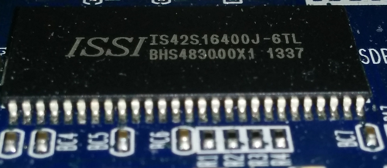
--- Quote Start --- sdram timing analysis The "KEY TIMING PARAMETERS" table has the relevant details. It says speed grade -5 when operated at a CAS latency of 3 has a minimum guaranteed operating frequency of 200MHz, but when you operate it with a CAS latency of 2 the minimum guaranteed operating frequency is 133MHz. You can interpret the other columns similarly. If you look at the package marking on the ISSI RAM on your board, you'll likely find that it has a -7 speed grade marking. --- Quote End --- Mine appears to be a -6 (see image attachment). That seems to imply that the sdram_controller clock needs to be 166MHz if the CAS latency cycles setting is set to 3. Do you agree? I still don't know which clock, the sdram_controller clock or the SDRAM_CLK out to the chip is supposed to be delayed. (Fine tuning how much it is delayed comes later). To try to answer that question, as you suggested, I attempted to look at the QSYS project you mentioned again since I edited the original compilation: synth.tcl compiles but in qsys_system you don't use a pll so that doesn't answer the question about the two different sdram clocks. qsys_system.tcl doesn't compile: "Error:can't find package qsys exactly 14.0" synth_qsys.tcl compiles but doesn't seem to do anything relevant. The qsys project file is the same as before. still no PLL. The other tcl files don't seem relevant to answering the question. So, that's done. Now would you be able to tell me which of the two clocks (the sdram_controller clock and/or the SDRAM_CLK out to the chip) is supposed to get the -3ns delay? I know it needs to be tuned with TimeQuest but a starting point would be nice. A second, more important issue, is whether or not the SDRAM chip is even fast enough to process 640 x 480 x 30fps x 2 (read + write) = 18,432,000 random read/write operations every second. Even at 100,000,000Hz you would think there would be plenty of time but maybe not with all of those other delays, pre-charges, etc going on.. Are 18.5 million random operations a second too much in your opinion?
- Mark as New
- Bookmark
- Subscribe
- Mute
- Subscribe to RSS Feed
- Permalink
- Report Inappropriate Content
--- Quote Start --- Mine appears to be a -6 (see image attachment). That seems to imply that the sdram_controller clock needs to be 166MHz if the CAS latency cycles setting is set to 3. Do you agree? --- Quote End --- No. The SDRAM clock can be slower than this. Once you get the SDRAM working at 100MHz, you can try to make it faster. Its quite possible that the FPGA speed grade is not fast enough to support 166MHz. Basically you'll have to try and see. --- Quote Start --- I still don't know which clock, the sdram_controller clock or the SDRAM_CLK out to the chip is supposed to be delayed. (Fine tuning how much it is delayed comes later). --- Quote End --- Its the clock to the external SDRAM devices that you adjust. You would see this if you looked at the DE0-nano SDRAM design. The PLL is instantiated outside the Qsys system at the top-level of the design. I did mention editing it with the MegaWizard ... --- Quote Start --- To try to answer that question, as you suggested, I attempted to look at the QSYS project you mentioned again since I edited the original compilation: synth.tcl compiles but in qsys_system you don't use a pll so that doesn't answer the question about the two different sdram clocks. qsys_system.tcl doesn't compile: "Error:can't find package qsys exactly 14.0" synth_qsys.tcl compiles but doesn't seem to do anything relevant. The qsys project file is the same as before. still no PLL. The other tcl files don't seem relevant to answering the question. --- Quote End --- Which version of Quartus are you using? The notes in the DE-nano SDRAM thread indicate I tested it under I tested it under Quartus 12.1, 13.0, 13.1, and 14.0. Perhaps you are using 14.? --- Quote Start --- So, that's done. Now would you be able to tell me which of the two clocks (the sdram_controller clock and/or the SDRAM_CLK out to the chip) is supposed to get the -3ns delay? I know it needs to be tuned with TimeQuest but a starting point would be nice. --- Quote End --- The clock to the SDRAM gets the delay. --- Quote Start --- A second, more important issue, is whether or not the SDRAM chip is even fast enough to process 640 x 480 x 30fps x 2 (read + write) = 18,432,000 random read/write operations every second. Even at 100,000,000Hz you would think there would be plenty of time but maybe not with all of those other delays, pre-charges, etc going on.. Are 18.5 million random operations a second too much in your opinion? --- Quote End --- No idea. That is why you need to simulate the design. The Altera SDRAM controller could be totally useless, but you will not know until to simulate a design with traffic that is representative of your design. Cheers, Dave
- Mark as New
- Bookmark
- Subscribe
- Mute
- Subscribe to RSS Feed
- Permalink
- Report Inappropriate Content
I've condensed the camera and vga entities so that there is a single, top level file for both.
When creating a new component in QSYS, I'm having trouble guessing which group needs to be selected. Any of the following seem like they could be right: Bridges and Adapters/Memory-Mapped, Bridges and Adapters/DMA, Bridges and Adapters/Streaming, Bridges/Memory-Mapped, Bridges/Streaming, or Qsys Interconnect/Memory-Mapped The camera basically outputs address, data, and write enable while the vga entity basically outputs an address and accepts pixel data. Which "group" best fits these two entities?Inst_ov7670_controller : entity work.ov7670_top PORT MAP(
clk => clk_camera,
resend => "not"(btn(2)),
config_finished => led(9), -- out
sioc => ov7670_sioc, -- out
siod => ov7670_siod, -- inout
reset => ov7670_reset,
pwdn => ov7670_pwdn,
xclk => ov7670_xclk,
pclk => ov7670_pclk,
rez_160x120 => rez_160x120,
rez_320x240 => rez_320x240,
vsync => ov7670_vsync,
href => ov7670_href,
d => ov7670_data,
addr => wraddress(18 downto 0), -- WRITE ADDRESS OUT -->
dout => wrdata(11 downto 0), -- WRITE DATA OUT -->
we => wren -- WRITE ENABLE OUT -->
);
Inst_VGA_controller : entity work.vga_top PORT MAP(
CLK25 => clk_vga,
rez_160x120 => rez_160x120,
rez_320x240 => rez_320x240,
Hsync => hsync, --out
Vsync => vsync, --out
Din => rddata(11 downto 0), -- <-- READ DATA INPUT
R => vga_r,
G => vga_g,
B => vga_b,
address => rdaddress(18 downto 0) -- READ ADDRESS OUT -->
);
- Mark as New
- Bookmark
- Subscribe
- Mute
- Subscribe to RSS Feed
- Permalink
- Report Inappropriate Content
--- Quote Start --- When creating a new component in QSYS, I'm having trouble guessing which group needs to be selected. --- Quote End --- That is not quite how creating a Qsys component works. You first have to determine *if* the bus interface used by your component is compatible with the Avalon-MM specification, i.e., whether its use of the address, read, write, and data correspond to the Avalon-MM use of those signal names. If it does not, then you have to create bridge logic that maps the transactions. That bridge might incorporate a FIFO (to handle bursts or latency). So my first question is, do you have a simulation for your VGA bus interface and your camera controller? If not, you should really write one :) Cheers, Dave
- Mark as New
- Bookmark
- Subscribe
- Mute
- Subscribe to RSS Feed
- Permalink
- Report Inappropriate Content
There are no packets or other data that can be reliably grouped or streamed. There are two different entities requesting to read and write from unpredictable addresses at unpredictable times usually simultaneously. So far I've created the QSYS component for the camera. I think I picked bridges and adapters/Avalon ST. It ended up being a memory master though after I set all of the parameters.. I messed up and made all the exports reside under one conduit name but other than that it might work.. I have a feeling I can't just connect the two masters to the SDRAM controller and trust that it will just 'figure' it out. There is probably some component that needs to handle that.. It would set priority like you mentioned earlier.. Any idea what component that would be? Maybe a frame buffer? I hope not because I want to be able to store and retrieve all sorts of other data using this SDRAM chip and random times..
- Mark as New
- Bookmark
- Subscribe
- Mute
- Subscribe to RSS Feed
- Permalink
- Report Inappropriate Content
--- Quote Start --- There are no packets or other data that can be reliably grouped or streamed. There are two different entities requesting to read and write from unpredictable addresses at unpredictable times usually simultaneously. --- Quote End --- But you call them camera and VGA interfaces. I would have thought they would work on frames of data. Based on your comments, the interfaces would not be implemented as Avalon-ST streams, but they do sound like they can be implemented as Avalon-MM master interfaces. --- Quote Start --- So far I've created the QSYS component for the camera. I think I picked bridges and adapters/Avalon ST. It ended up being a memory master though after I set all of the parameters.. I messed up and made all the exports reside under one conduit name but other than that it might work.. I have a feeling I can't just connect the two masters to the SDRAM controller and trust that it will just 'figure' it out. --- Quote End --- Yes, you can. So long as the two masters implement the Avalon-MM protocol correctly, then read and writes should work fine. You would use your simulation to determine if the default arbitration shares are appropriate, or whether you need to change them. --- Quote Start --- There is probably some component that needs to handle that.. It would set priority like you mentioned earlier.. Any idea what component that would be? --- Quote End --- Stop making me repeat myself. If you're not going to read the documentation on Qsys, arbitration, and arbitration shares, then I'll just stop responding to this thread. --- Quote Start --- Maybe a frame buffer? I hope not because I want to be able to store and retrieve all sorts of other data using this SDRAM chip and random times.. --- Quote End --- This is what you need a simulation to determine. If data read pre-fetching or write-posting is appropriate in your design, then a buffer between your devices and the SDRAM might be sufficient. This buffering would be most efficient if your data transfers occur in blocks, but you make it sound like that is not the case. Cheers, Dave
- Mark as New
- Bookmark
- Subscribe
- Mute
- Subscribe to RSS Feed
- Permalink
- Report Inappropriate Content
I'll read up on arbitration.
What's going on is the camera entity has it's own clock and is just churning out address + data values that represent the pixel locations and pixel colors that it sees. It can't wait, or buffer, or anything. I'll probably have to use a FIFO memory component that uses the FPGA's limited memory. The vga_out entity is doing the same thing at it's own independent clock rate except that it is asking for pixel data for a given address location. Both entities read and write to the same address space for now. They also often request SDRAM access at the same time. I can't just have it wait until a complete frame is written to memory because that will interfere with the display image. What I really need is the closest thing possible to a 2-port RAM.- Mark as New
- Bookmark
- Subscribe
- Mute
- Subscribe to RSS Feed
- Permalink
- Report Inappropriate Content
--- Quote Start --- What I really need is the closest thing possible to a 2-port RAM. --- Quote End --- So why not use a board with QDR II+ SRAM then? The bottom-line is you have no hope of any sort of success without simulating your design. You need a simulation of how your camera interface works and how your VGA interface works. With those two simulations, you can determine if you can map them as Avalon-MM bridges, or if you can convert them to streaming interfaces. Then you can determined the memory interface requirements, so that you an determined whether you can use SDRAM or you require QDR II+ SRAM. SDRAM is good for bursts, not as good for random accesses, but it can implement large memories and cheap. QDR II+ SRAM is good for random access, but its small and expensive. Cheers, Dave
- Mark as New
- Bookmark
- Subscribe
- Mute
- Subscribe to RSS Feed
- Permalink
- Report Inappropriate Content
I see. I can't really run simulations currently because of modelsim's sinlge-HDL restriction. I'll have to find a way around that..
There is an upside of lower cost if SDRAM ends up working out though. These will replace our current products if I ever get that far with it. Getting a clean 640x480 image is only step one in a 30+ step development process. As of writing this, the entire system is QSYS-based. The image has lost all of its noise but now has an interlaced-look to it (see attached image). QSYS did automatically create a FIFO, among other things, automatically which was nice. I now have to take wild guesses as to what is causing that interlaced look.. The camera and VGA entity ended up as "Bridges and Adapters/Streaming" modules which have Avalon Memory Mapped Master interfaces. One category of settings which is very likely to be wrong are the ones in the attached image. Do any of those stand out as definitely wrong to you? I don't know what "bits per symbol" is in this context. I'll have to look into that... UPDATE: It has a combination of pixelation, as if a 20x20 square is treated as one block, and an interlaced effect which gets worse as I slow the clock down from a starting point of 166MHz- Mark as New
- Bookmark
- Subscribe
- Mute
- Subscribe to RSS Feed
- Permalink
- Report Inappropriate Content
--- Quote Start --- I can't really run simulations currently because of modelsim's sinlge-HDL restriction. I'll have to find a way around that.. --- Quote End --- Modelsim can handle multiple languages. I use Modelsim-SE. Modelsim-Altera Edition appears only to support a single language: https://www.altera.com/products/design-software/model---simulation/modelsim-altera-software.html --- Quote Start --- There is an upside of lower cost if SDRAM ends up working out though. These will replace our current products if I ever get that far with it. --- Quote End --- Sure, but you need to exhaustively test your code to ensure that SDRAM can meet that requirement, and you cannot do that without proper simulation tools. --- Quote Start --- Getting a clean 640x480 image is only step one in a 30+ step development process. --- Quote End --- And without proper simulation, you're stumbling at step 1. --- Quote Start --- As of writing this, the entire system is QSYS-based. --- Quote End --- You have yet to convince me that you are using Qsys correctly. Just mapping your camera and VGA ports to seemingly identically names ports in Qsys does not make them Avalon-MM components. --- Quote Start --- I now have to take wild guesses as to what is causing that interlaced look.. --- Quote End --- No, you don't. You simulate and you understand, there's no need to guess about anything. --- Quote Start --- The camera and VGA entity ended up as "Bridges and Adapters/Streaming" modules which have Avalon Memory Mapped Master interfaces. --- Quote End --- You're just showing your lack of understanding here. That is just a "section" in the IP catalog. It means nothing. I'm going to stop responding to this thread until you post a simulation of your VGA and camera interfaces showing that they implement Avalon-MM master interfaces. Modelsim Altera Starter Edition is free, and you should be able to take your existing single-language code and either convince me the interfaces can be mapped to Avalon-MM interfaces or already adhere to the Avalon-MM requirements. Good luck! Cheers, Dave
- Mark as New
- Bookmark
- Subscribe
- Mute
- Subscribe to RSS Feed
- Permalink
- Report Inappropriate Content
I have modelsim 10.1c SE installed and a testbench made but I need a SDRAM simulation model. Any idea what the detailed steps are to get one set up in modelsim?
# This reference design requires a vendor simulation model.
#  To simulate accesses to SDRAM, you must:
#        - Download the vendor model
#        - Install the model in the system_sim directory
#        - Add the vendor file to the list of files passed to 'vcom' in setup_sim.do
#        - Instantiate sdram simulation models and wire them to testbench signals
#        - Be aware that you may have to disable some timing checks in the vendor model
#               (because this simulation is zero-delay based)
- Mark as New
- Bookmark
- Subscribe
- Mute
- Subscribe to RSS Feed
- Permalink
- Report Inappropriate Content
--- Quote Start --- I have modelsim 10.1c SE installed and a testbench made but I need a SDRAM simulation model. Any idea what the detailed steps are to get one set up in modelsim? --- Quote End --- Its quite possible that Altera has one for you. I'm pretty sure that the newer versions of Qsys have an option to create an example testbench design. I've used it with the DDR controller, and that includes a DDR model. Try and see if that scheme works with SDRAM too. Run the DE0-nano Qsys design and from within Qsys have it generate an example project. I just tried this with 12.1sp1, and the feature to create an example does not exist in that version. I don't have time to try another version right now, so you should go ahead and see if that feature works for an SDRAM model. If it does not, you can download models from ISSI or Micron's web site. The ISSI SDRAM is just a clone of some Micron model, you'll just have to find out which. ISSI probably has a "replacement part for Micron" list somewhere. Cheers, Dave
- Mark as New
- Bookmark
- Subscribe
- Mute
- Subscribe to RSS Feed
- Permalink
- Report Inappropriate Content
I have Quartus 13.1 since it is the last version that supports the Cyclone III used in the DE0.
Yes, QSYS may have generated one when I told it to generate the simulation or test bench. What am I looking for though? What is the file extension or likely file name? Once I find it, is it just added to a modelsim project like a vhdl file or is there a different import process?- Subscribe to RSS Feed
- Mark Topic as New
- Mark Topic as Read
- Float this Topic for Current User
- Bookmark
- Subscribe
- Printer Friendly Page