- Mark as New
- Bookmark
- Subscribe
- Mute
- Subscribe to RSS Feed
- Permalink
- Report Inappropriate Content
I am trying to use AN756 to understand how to implement a 300 MHz (single data rate) source-synchronous input data interface.
I previously tried to infer ordinary GPIO for this interface, but it fails timing. My target device is a Cyclone 10 GX 10CX085.
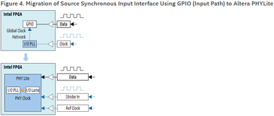
AN756 only provides this diagram (and no accompanying text to explain what it means):
After much searching and reading online, my understanding is the following:
- The external (source-synchronous) clock must be connected to StrobeIn.
- This clock must be routed (on the PCB) to a specific x8/x9 DQS pin on the FPGA.
- The source-synchronous data must be routed (on the PCB) to the same DQ group as StrobeIn's DQS.
- An additional RefClock must be provided.
- Best jitter performance is usually achievable if this is an external clock.
- The RefClock frequency must be selected from a specific list. (Ideally it is exactly half the StrobeIn frequency).
- Both reset_n and rdata_en can be held high in this use case.
Therefore, if my source-synchronous clock and data are named Clk_In and Data_In, then I think I can basically convert these to Clk_Core and Data_Core like this (in VHDL):
    i_phylite : component phylite
    port map (
        ref_clk              => Clk_Ref,
        reset_n              => '1',
        interface_locked     => open,
        core_clk_out         => Clk_Core,
        group_0_data_to_core => Data_Core,
        group_0_rdata_en     => (others => '1'),
        group_0_rdata_valid  => open,
        group_0_data_in      => Data_In,
        group_0_strobe_in    => Clk_In
    );
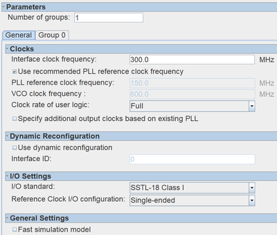
As far as I can see, the "General" configuration is fairly straightforward:
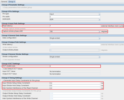
However the "Group 0" configuration is a bit more confusing. There are 4 parts I would like help with:
- What does "Read latency" mean in this context? (I am not reading anything from anywhere).
- My source-synchronous data is center-aligned (it is stable around the rising edge of the source-synchronous clock). Does this mean I should set the "Capture strobe phase shift" to 180 degrees?
- Do I need a nonzero "OCT enable size"?
- In the "Timing Settings", can I just enter the setup and hold times specified in the datasheet of the external device (which is outputting the source-synchronous input to the FPGA)?
Apart from this, have I generally understood how to use the PHY Lite IP correctly? This requires hardware (PCB) changes, so I would like to get it right.
- Mark as New
- Bookmark
- Subscribe
- Mute
- Subscribe to RSS Feed
- Permalink
- Report Inappropriate Content
I reopened this topic here, but still received no useful help from the "community" staff.
My company was somehow able to contact an engineer at Intel, who solved the problem immediately.
In summary:
- The refclk and strb pins (two FPGA pins) must both be driven by the same external clock.
- There is a bug in all versions of Quartus up to and including 21.4, which prevents the IO delay chains from being configured correctly. Therefore, the design will typically fail timing, even if everything has been configured correctly. As a workaround (until the bug is fixed in Quartus 22.1), the IO delay chains can be configured manually (see details below).
Here is the content of the (excellent) E-mail:
Quartus should automatically change the IO delay chain settings such that each IO is optimized for both setup and hold however there appears to be a problem with the automatic delay chain calculation algorithm in 21.3 which is why you are seeing lots of hold violations while your setup looks good.

I have checked in 21.4 and can confirm that the same issue exists in that version too.
I can however confirm that this issue has been resolved in the latest internal release of 22.1 which is due for release very soon.

As a temporary solution (prior to the release of 22.1) you can manually set the IO delay chain values using the assignment below.

set_instance_assignment -name IO_12_LANE_INPUT_DATA_DELAY_CHAIN 60 -to InData

You can apply this to all InData pins (as in the assignment above) however to get the optimum solution you will need to apply different values on a per-pin basis which is also supported.
I am looking at what specific settings are required to close timing and will update you in due course.

You can see the delay chain values used in the "Delay Chain Summary" section of the Route Stage report.

I tested the assignment above in 21.3 and the interface closed timing.

With regard to the refclk versus the strobe, ideally these should both originate from the same clock source such that they are PPM aligned. This will prevent the internal FIFO within the PHYLITE IP from overflowing/underflowing.
The simplest solution is to connect the same clock on your board to both the strobe and refclk pins of the device.
We applied these changes in our project and it met timing. Correct behavior has been confirmed in simulation.
Link Copied
- Mark as New
- Bookmark
- Subscribe
- Mute
- Subscribe to RSS Feed
- Permalink
- Report Inappropriate Content
Hi Harry,
Happy New Year!
I'm sorry for some delay in responding to you.
May I know which Quartus version that you're using?
Regards,
Adzim
- Mark as New
- Bookmark
- Subscribe
- Mute
- Subscribe to RSS Feed
- Permalink
- Report Inappropriate Content
@AdzimZM_Intel I would be happy to use any version of Quartus, if some versions work but others don't. Is that the case?
I'm currently trying to use Quartus Prime Version 21.1.0 Build 169 03/24/2021 SC Pro Edition.
- Mark as New
- Bookmark
- Subscribe
- Mute
- Subscribe to RSS Feed
- Permalink
- Report Inappropriate Content
Hi,
You may want to refer to AN 433: https://cdrdv2.intel.com/v1/dl/getContent/653688?explicitVersion=true&wapkw=An%20433, page 39.
Regards
- Mark as New
- Bookmark
- Subscribe
- Mute
- Subscribe to RSS Feed
- Permalink
- Report Inappropriate Content
@Ash_R_Intel That link is nothing to do with PHY Lite.
The reason I need to use PHY Lite is that the normal practice described in AN 433 fails timing.
- Mark as New
- Bookmark
- Subscribe
- Mute
- Subscribe to RSS Feed
- Permalink
- Report Inappropriate Content
Hi,
Have you checked the PHY Lite for Parallel Interfaces Intel® FPGA IP User Guide: https://www.intel.com/content/www/us/en/docs/programmable/683716/21-4/about-the-ip.html ?
All your queries related to PHY Lite IP are answered there.
Regards
- Mark as New
- Bookmark
- Subscribe
- Mute
- Subscribe to RSS Feed
- Permalink
- Report Inappropriate Content
@Ash_R_Intel Yes, I have read through the PHY Lite user guide in detail several times.
Could you clarify which part(s) you think answer my questions?
- Mark as New
- Bookmark
- Subscribe
- Mute
- Subscribe to RSS Feed
- Permalink
- Report Inappropriate Content
Hi,
Any update from your end? Did the user guide answer all your queries?
Regards
- Mark as New
- Bookmark
- Subscribe
- Mute
- Subscribe to RSS Feed
- Permalink
- Report Inappropriate Content
Hi,
Do you still need support on this issue? Was the User guide helpful to clear your doubts? Please confirm.
Regards
- Mark as New
- Bookmark
- Subscribe
- Mute
- Subscribe to RSS Feed
- Permalink
- Report Inappropriate Content
@Ash_R_Intel Yes, I still need help, as my questions have not been answered. If you think the user guide answers my questions, then please clarify which parts answer my questions. I have spent many hours reading through it and I couldn't find any of the information I was looking for.
- Mark as New
- Bookmark
- Subscribe
- Mute
- Subscribe to RSS Feed
- Permalink
- Report Inappropriate Content
Hi,
Please refer 4.3.1. Parameter Settings, Table 75, for description on all the parameters in the IP wizard. https://www.intel.com/content/www/us/en/docs/programmable/683716/21-4/parameter-settings-36186.html
Additionally, some more info available in same document.
Read Latency : Refer section 4.2.4 Input Path, Table 62, Read and Strobe Enable Path and Figure 66, block VFIFO. This parameter affects the rdata_valid signal assertion.
Capture Strobe Phase shift : Refer section 4.2.4 Input Path, Table 62, Strobe path and Figure 66, Delay Chain (PVT) in blue color. This parameter aligns the phase of the dqs input with respect to data.
Regards
- Mark as New
- Bookmark
- Subscribe
- Mute
- Subscribe to RSS Feed
- Permalink
- Report Inappropriate Content
We do not receive any response from you to the previous answer that I have provided. This thread will be transitioned to community support. If you have a new question, feel free to open a new thread to get the support from Intel experts. Otherwise, the community users will continue to help you on this thread. Thank you
- Mark as New
- Bookmark
- Subscribe
- Mute
- Subscribe to RSS Feed
- Permalink
- Report Inappropriate Content
I reopened this topic here, but still received no useful help from the "community" staff.
My company was somehow able to contact an engineer at Intel, who solved the problem immediately.
In summary:
- The refclk and strb pins (two FPGA pins) must both be driven by the same external clock.
- There is a bug in all versions of Quartus up to and including 21.4, which prevents the IO delay chains from being configured correctly. Therefore, the design will typically fail timing, even if everything has been configured correctly. As a workaround (until the bug is fixed in Quartus 22.1), the IO delay chains can be configured manually (see details below).
Here is the content of the (excellent) E-mail:
Quartus should automatically change the IO delay chain settings such that each IO is optimized for both setup and hold however there appears to be a problem with the automatic delay chain calculation algorithm in 21.3 which is why you are seeing lots of hold violations while your setup looks good.

I have checked in 21.4 and can confirm that the same issue exists in that version too.
I can however confirm that this issue has been resolved in the latest internal release of 22.1 which is due for release very soon.

As a temporary solution (prior to the release of 22.1) you can manually set the IO delay chain values using the assignment below.

set_instance_assignment -name IO_12_LANE_INPUT_DATA_DELAY_CHAIN 60 -to InData

You can apply this to all InData pins (as in the assignment above) however to get the optimum solution you will need to apply different values on a per-pin basis which is also supported.
I am looking at what specific settings are required to close timing and will update you in due course.

You can see the delay chain values used in the "Delay Chain Summary" section of the Route Stage report.

I tested the assignment above in 21.3 and the interface closed timing.

With regard to the refclk versus the strobe, ideally these should both originate from the same clock source such that they are PPM aligned. This will prevent the internal FIFO within the PHYLITE IP from overflowing/underflowing.
The simplest solution is to connect the same clock on your board to both the strobe and refclk pins of the device.
We applied these changes in our project and it met timing. Correct behavior has been confirmed in simulation.
- Subscribe to RSS Feed
- Mark Topic as New
- Mark Topic as Read
- Float this Topic for Current User
- Bookmark
- Subscribe
- Printer Friendly Page


