- Marcar como nuevo
- Favorito
- Suscribir
- Silenciar
- Suscribirse a un feed RSS
- Resaltar
- Imprimir
- Informe de contenido inapropiado
We need to integrate PCIe Gen2x1 and DDR3 via DMA. So we generated a PCIe Gen2x1 and we tried to add PCIE DMA Controller 64 and Avlon MM clock crossing bridge to access DDR3 memory of 2G space. But while generating testbench we are getting the error on differences in address mapping. While we are trying address 2GB of data, testbench is trying to address 4GB and we get a mismatch in address range. Could you please check these issues?.
I have attached the project file and screen error screen shot for your reference.
- Marcar como nuevo
- Favorito
- Suscribir
- Silenciar
- Suscribirse a un feed RSS
- Resaltar
- Imprimir
- Informe de contenido inapropiado
Hello Sir,
The reason is that you export the master port of the clock crossing bridge. And the BFM in default will generate the address 32bits. What you need to do is add the BFM slave manually and set the address to 30bits. And turn on the burst on burst boundaries only option. Then connect the CC bridge and the BFM slave clock and reset from the system. With this. The testbench can generate correctly. Attach the modified qsys file.
Enlace copiado
- Marcar como nuevo
- Favorito
- Suscribir
- Silenciar
- Suscribirse a un feed RSS
- Resaltar
- Imprimir
- Informe de contenido inapropiado
Hello Sir,
The reason is that you export the master port of the clock crossing bridge. And the BFM in default will generate the address 32bits. What you need to do is add the BFM slave manually and set the address to 30bits. And turn on the burst on burst boundaries only option. Then connect the CC bridge and the BFM slave clock and reset from the system. With this. The testbench can generate correctly. Attach the modified qsys file.
- Marcar como nuevo
- Favorito
- Suscribir
- Silenciar
- Suscribirse a un feed RSS
- Resaltar
- Imprimir
- Informe de contenido inapropiado
Hi,
Thank you for your response. We added the Avalon-MM slave BFM and set the parameters as advised by you and we were able to successfully create testbench system for the design.
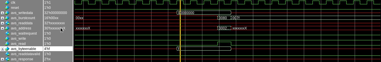
We could see a read transaction in the Avalon MM slave BFM but the Read response is always driven as X. Attached is the screenshot for the same. Could you please let us know how to proceed with this?
I will also add the QSYS file of the design for your reference.
- Marcar como nuevo
- Favorito
- Suscribir
- Silenciar
- Suscribirse a un feed RSS
- Resaltar
- Imprimir
- Informe de contenido inapropiado
Hello,
The BFM component in platform design maybe is genric and unable to show full functionality.
Are you want to run the simulation for PCIe? If yes, maybe you can use the PCIe example design as explained in this UG:
https://www.intel.com/content/dam/www/programmable/us/en/pdfs/literature/ug/ug-dex-a10-pcie-avst.pdf
- Marcar como nuevo
- Favorito
- Suscribir
- Silenciar
- Suscribirse a un feed RSS
- Resaltar
- Imprimir
- Informe de contenido inapropiado
Thank you for the support.
We were able to do DDR3 memory access.
Regards,
Sudhir
- Marcar como nuevo
- Favorito
- Suscribir
- Silenciar
- Suscribirse a un feed RSS
- Resaltar
- Imprimir
- Informe de contenido inapropiado
Good to know. Thanks.
- Marcar como nuevo
- Favorito
- Suscribir
- Silenciar
- Suscribirse a un feed RSS
- Resaltar
- Imprimir
- Informe de contenido inapropiado
I’m glad that your question has been addressed, I now transition this thread to community support. If you have a new question, feel free to open a new thread to get the support from Intel experts. Otherwise, the community users will continue to help you on this thread. Thank you.
- Suscribirse a un feed RSS
- Marcar tema como nuevo
- Marcar tema como leído
- Flotar este Tema para el usuario actual
- Favorito
- Suscribir
- Página de impresión sencilla